Facebook
 Google
 GitHub
 Linkedin
Driving SiC MOSFETs with a HighSpeed Gate Driver IC
Silicon-Carbide (SiC) MOSFETs that become a visible part of the MOSFET market require special gate drivers that are able to provide a negative voltage
Silicon-Carbide (SiC) MOSFETs that become a visible part of the MOSFET market require special gate drivers that are able to provide a negative voltage to the gate in a MOSFETs off state, high charge/discharge pulse current, and are fast enough to operate gate in the nanoseconds range. The IC IX6611, an intelligent high-speed gate driver, can be easily used to drive silicon-carbide (SiC) MOSFETs as well as standard MOSFETs and IGBTs.
The IX6611 provides negative voltage to the gate from zero to minus 10V and positive voltage from 12V to 25V as long as the difference between negative and positive voltage does not exceed 30V. It is able to provide up to ±10A gate charge/discharge current with identical 50ns propagation delay for falling and rising pulse edges that prevents pulse distortion. The IX6611 contains the necessary circuit blocks for the pulse transformer isolated applications that allow galvanically isolate a signal source/recipient like microcontroller unit (MCU) from high power circuitry maintaining bi-directional communication. That provides the MCU necessary feedback signals in case of a fault.
It also implements monitor/protection functions such as supply under- and over-voltage lockout, thermal shutdown, as well as switching device over-current and over-voltage protection. It is designed to operate over a temperature range of -40°C to +125°C, and it is available in a 16-Lead SOIC with exposed pad.
The IX6611 Features
The IX6611 has the following features:
- Signal inputs/outputs are compatible with pulse transformer to communicate with galvanically isolated MCU
- 10 A peak source and sink current gate drive with separate source and sink outputs
- Negative gate drive capability to drive IGBTs or SiC MOSFETs.
- Overcurrent protection with adjustable blanking time.
- Advanced active clamping protection
- Under- and over-voltage lockout protection.
- Two 1 Amperes pulse transformer drivers for fault signals communication.
The IX6611 is designed to provide gate drive for high power switching devices converting the incoming PWM logic signals into +15 V/-5 V (in respect to COMMON) bi-polar gate drive signal with a typical ±10 A peak drive current capability. Separate positive and negative gate driver outputs allow optimize turn on/off time without an external diode selecting serial gate resistors of the different value (See Figure 1a, resistors R1 and R2). Internal dead time circuit eliminates the cross conduction of the source and sinks outputs.
If negative offset for gate voltage not required, VEE and PVEE inputs should be tied to COMMON. In this case, a negative voltage source is not used; internal logic is powered from an internal VDD source. VCC voltage should be at least 5 V above UVLO threshold shown in the datasheet to avoid UVLO condition detect. An Over Current Comparator with a 300 mV threshold in respect to COMMON, is designed to sense the overcurrent conditions. The current sense can be implemented either by using a low-value current sense resistor, a MOSFET/IGBT with a secondary current sense output, or de-saturation event (see figures 1a, 1b, and 2).
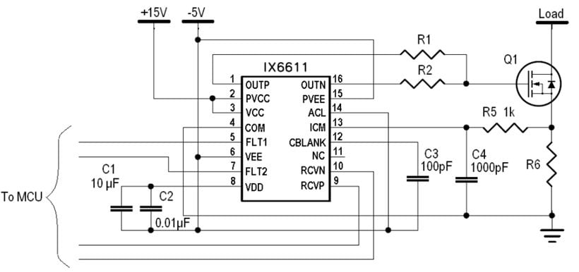
Figure 1a: Over-current protection using IX6611 ICM comparator and current sense resistor.
Overcurrent Fault Protection
If an overcurrent fault occurs, the driver’s output is forced low for the remainder of the cycle. Normal operation resumes at the beginning of the next PWM gate drive cycle.
A noise filter (R5C4) at the current sense input may be required due to low sense voltage.
When an overcurrent occurs, the Output Faults Pulse Generator creates a narrow 200ns pulse that is used by the Fault Control Logic to communicate the fault condition to the MCU.
The OC comparator’s input is grounded during the off time of the switching device and remains grounded for a fixed amount of time immediately after switching device turns on to prevent false tripping. Leading Edge Blanking Circuit sets the blanking time, which is programmable by an external capacitor (See Figure 1a, capacitor C3).

Figure 1b: Over-current protection using IX6611 ICM comparator, current sense resistor, and an additional comparator.
Power Dissipation
If power dissipated on a current sense resistor is too high or it is difficult to find current sense resistor with the appropriate value for current limiting, an additional comparator can be used as shown on Figure 2b. In this case, precision adjustment for desirable current is possible with relatively small power dissipation on current sense resistor.
Traditional de-saturation protection for IGBTs or protection triggered by high voltage drop on RDC_ON for SiC MOSFETs can also be implemented using a large ratio resistive divider across drain to source (See Figure 2). Resistive divider R13/R14 has two limitations regarding its value. The voltage drop across R14 should be above 300mV to trigger ICM comparator in case of the desaturation event/high voltage drop on RDC_ON, and it should not load high voltage source when switching device is in off state. The minimum divider’s current should be above 1µA to prevent an influence of the ICM input current. Resistor R13 is usually a serial connection of low voltage cheap resistors like standard 1206 SMD resistors with 500V rating. The number of resistors in series should be the next integer above drain/collector voltage divided by 500V.
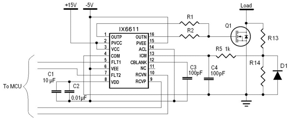
Figure 2: Over-current protection using IX6611 ICM comparator and de-saturation voltage.
Resistor R5 is used for noise filtering purposes only and it can be omitted with proper power board design. Otherwise, it should locate as close to ICM pin as possible. Diode D1 is used to protect a driver from negative voltage spikes and should be a fast forward recovery one with a low capacitance like 1N4448HWS-7-F from Diodes Incorporation.
Capacitor C4 is shorted by 2 kOhms switches inside IX6611 when switching device gate voltage is negative. The switch allows C4 start charging after gate voltage goes high and blanking time set by capacitor C3 expires. If shorter response time for de-saturation event requires, C3 and C4 capacitors value can be reduced at expense to lower system noise immunity.
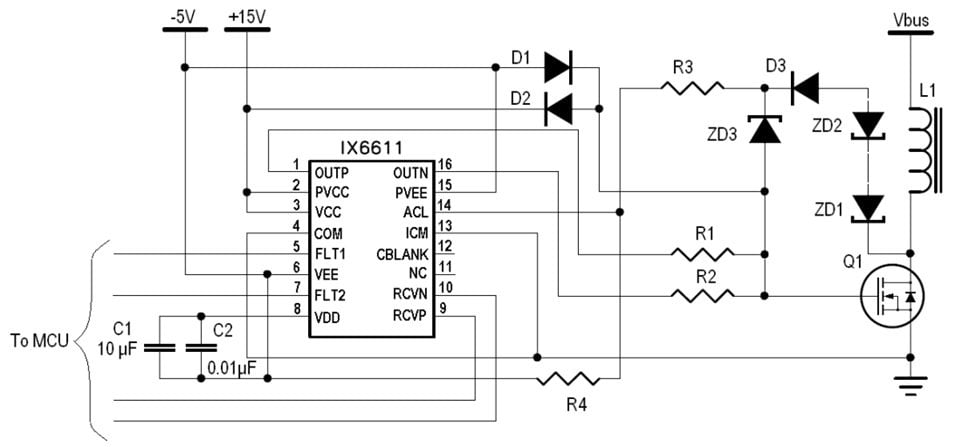
Figure 3: Active clamping using IX6611 ACL comparator.
Active Clamping protection is used to protect the switching device from the over-voltage condition at the drain/collector when an inductive load is turned off with high current. If ACL comparator is triggered, it allows keeping switching device conducting until the energy stored in the inductor will be not enough to create collector over-voltage condition.
ACL Comparator
The IX6611 utilizes ACL comparator with 3.1 V threshold in respect to the negative gate voltage source (VEE) that may be used for implementing an advanced active clamping technique as shown in application circuit diagram (Figure 3). The ACL comparator monitors the voltage at resistive divider R3/R4, which is connected to IGBT collector through clamp diodes ZD1, ZD2. If IGBT collector voltage exceeds value equal VZD1 + VZD2 + VZD3 + VEE threshold, current starts flowing into OUTN gate driver output creating a voltage drop across ZD3. The resistive divider should be chosen such way that voltage drop across R4 exceeds ACL comparator threshold of 3.1 V, i.e. VZD3*R4 / (R3 + R4) > 3.1 V in respect to VEE. Triggering the ACL comparator forces the gate driver output to a tri-state condition and the IGBT starts to turn on due to the breakdown diode current charging the IGBT gate.
Once the IGBT turns on, its collector voltage falls, the diode recovers from a breakdown, and the ACL comparator turns on the OUTN output, which forces the IGBT gate low. This sequence may repeat several times until the energy in the external inductance is dissipated. ACL comparator is active only when the driver’s output OUTP is OFF. Normal operations resume at the beginning of the next PWM gate drive cycle.
Diodes D1, D2 protect IGBT gate from over-voltage in case of the voltage at the IGBT gate becomes more positive than VCC or more negative than VEE. Diode D3 protects gate driver OUTP output from draining current into the collector when it becomes less positive than VCC.
This technique is rarely used with MOSFETs and, if this function not required, it may be easily disabled by connecting ACL comparator’s input to VEE pin.
The IX6611 contains Under- and Over-voltage Lockout Comparators (UVLO and OVLO respectively) that monitor the positive power supply terminal. If at the beginning of the PWM pulse positive power supply voltage is below UVLO threshold or above OVLO threshold, the gate driver output is driven low and it skips that PWM pulse. However, if UVLO or OVLO conditions occur after PWM pulse start, these conditions are ignored until next PWM pulse coming.
If the positive power supply recovers from the fault condition, the normal operation resumes on the next PWM pulse. The UVLO circuit becomes operational at VCC above 3V and keeps the gate driver output low until VCC raises above the UVLO threshold.
Fault Information Communication
Fault information is communicated to the MCU as narrow pulses. Based on the type of fault, the fault control logic selects narrow pulses either from the input interface or from the output fault pulse generator.
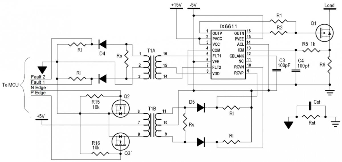
Figure 4: MCU connection with IX6611 using an isolation transformer.
UVLO fault condition is communicated to the MCU as FLT1 pulse that is an input interface pulse representing the leading edge of the PWM pulse delayed by IX6611 propagation delay time. OVLO fault condition is communicated to the MCU as FLT2 pulse that is an input interface pulse representing the trailing edge of the PWM pulse also delayed by IX6611 propagation delay time. The IGBT Over-current condition is communicated to the MCU as FLT2 pulse from the internal output fault pulse generator, which is synchronized with an Over-current event, but not leading/trailing edges of the input PWM signal. FLT1 and FLT2 outputs are of open drain architecture and are capable of sinking up to 1 A current. The IX6611 input interface is working in start/stop mode with a short positive pulse signal at the RCVP input representing the leading edge of the PWM pulse and short positive pulse at RCVN input representing a falling edge of the PWM pulse. The IX6611 pulse recovery logic reconstructs PWM pulse and generates complementary signals at OUTP/OUTN outputs.
Leading/trailing edge pulses can be as short as 100 ns minimum. This allows the use of either direct MCU connection with a driver, or isolation transformers with small volt-second value to transmit PWM pulses with duration from 200 ns to infinity. So, the IX6611 may be used not only for fast switching applications like motor drivers, DC/DC bust converters, or AC/DC PFC converters but for switches of high power devices operating once per day and so on.
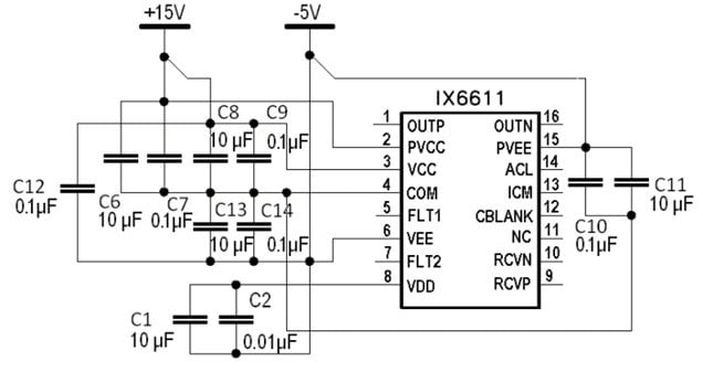
Figure 5: Recommended decoupling for IX6611 driving MOSFET.
RCVP/RCVN logic inputs threshold is more than 2.2 V for logic “one” and less than 1.0 V for logic “zero”. To reject noise and high-frequency interference a well-matched full differential architecture is used at receivers with 1 V hysteresis Schmitt Trigger buffers. That allows direct connection of the MCU to the gate driver in case of MOSFET as gate driver load with VEE/PVEE and COMMON pins tied together. Gate driver inputs are of high impedance, so MCU outputs should be configured as low current outputs, while MCU inputs receiving information about fault condition should be configured as pull-up inputs. If the IX6611 is used to drive SiC MOSFET or IGBT and negative voltage source required, logic signals should be transmitted and received in respect to negative VEE source that requires MCU ground to be connected to a negative voltage source. It may be not convenient or not possible. In such cases, an isolation transformer should be used to separate MCU and driver. That allows also galvanically isolate MCU from IX6611 and high power device significantly increasing MCU noise immunity in high power applications.
Input Interface to the gate driver is designed to be compatible with pulse transformers with small volt-second value like standard Ethernet/10Base-T isolation transformers PE-68023, PE-65745, PE65454, or similar.
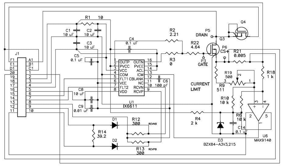
Figure 6: Schematic of the SiC MOSFET test board used for the two-pulse test with IX6611 as a gate driver and additional comparator to set different maximum drain current values using the same current sense resistor.
Recommended MCU/gate driver connection with isolation transformer is shown in Figure 4.
If MCU outputs are of low current capability, additional MOSFETs (Q2, Q3) should be used to drive transformer. It is recommended to use windings with ratio 1:1.41 or 1:2 to improve noise immunity on the driver’s (secondary) side, especially if MCU is of low voltage like 3.3 V or less.
Also, attention should be paid on fault signals at MCU inputs, which should not exceed MCU limits, because IX6611 drive transformer’s winding with ~5 V.
Shunt resistor Rs is used to prevent the transformer’s winding from ringing on parasitic capacitance, which may create false triggering on the input of opposite polarity. Its value should be in the range from 20 Ω to 50 Ω. Diode matrix D4, D5 with low forward voltage form positive pulse only on load resistors Rl, from which IX6611 and MCU read information. Recommended Rl resistors value should be in the range from 50 Ω to 500 Ω to maximize noise immunity. The decreasing value of Rs and Rl resistors increases noise immunity but also increases the load on the transformer’s primary side winding.
To avoid static electricity accumulation, high voltage low capacitance (220 pF – 470 pF) capacitor and/or 2 – 5 MΩ resistors should be installed between IX6611 COMMON and MCU ground plane as shown in Figure 4 (Cst, Rst).
Thermal Shutdown Circuit
The IX6611 contains a Thermal Shutdown circuit to protect the device against the damage due to excessive die temperature. When the junction temperature exceeds 150°C, the input signals to the gate driver and the ACL comparator are disabled and the gate driver output is forced low. Device resumes normal operation when the junction temperature falls below 130°C. It is recommended to solder package bottom pad to the pad on PCB tied to VEE to improve package power dissipation.
The IX6611 is a high frequency high current driver operating at a very noisy environment like high power motors, inductors, heaters, and other heavy industrial equipment. So, close attention should be paid to PCB layout to maximize noise immunity and driver’s performance.
Figure 5 depictures recommended decoupling schematic for IX6611 driving SiC MOSFET. It is recommended to split decoupling capacitors between VCC and PVCC pins and locate them as close to the pins as possible. Noise filtering capacitor C3 should locate as close to the ICM input as possible to improve noise immunity. Ground plane should be connected to COMMON and tied to the high current circuit at one point only to avoid high current flowing under IX6611.
The internal VDD regulator provides power to the internal low voltage circuits that are referenced to VEE. The regulator is powered from VCC in respect to VEE and its output voltage is referenced to VEE. External bypass capacitors C1, C2 accommodate transient currents.
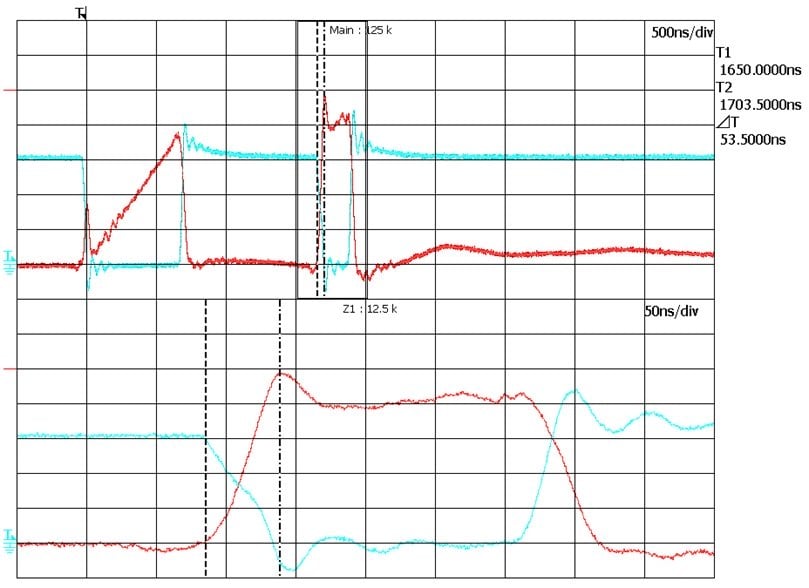
Figure 7: The IXYS Corporation SiC MOSFET IXFN70N120SK performance with IX6611 gate driver at Vds = 600 V and Id = 20 A. Channel 1 – red – drain current (5 A/div), channel 4 – blue – drain voltage (200 V/div).
Figure 6 demonstrates schematic of the SiC MOSFET test board used for the two-pulse test with the IX6611 as a gate driver and additional comparator to set different maximum drain current values using the same current sense resistor. Figure 7 shows performance of the IXYS Corporation SiC MOSFET IXFN70N120SK at Vds = 600 V and Id = 20 A.
About the Authors
Leonid Neyman is a Senior Applications Manager at IXYS Corporation. Abdus Sattar, Ph.D., is the Director of Engineering at Littelfuse.