Facebook
 Google
 GitHub
 Linkedin
Compact SiC Module for High Power Density On-Board Chargers
Today’s on-board chargers (OBCs) can benefit from lighter and more efficient electronic components. Learn how compact transfer molded power modules meet these needs.
This article is published by EEPower as part of an exclusive digital content partnership with Bodo’s Power Systems.
Article co-authored by Christian Felgemacher, Rohm Semicondcutor.
Development in the field of electromobility is progressing rapidly: electric powertrain systems are becoming ever more efficient and compact to increase vehicle autonomy and the range. An essential part of this development is the on-board charger (OBC), which must be highly efficient and at the same time have as little weight and volume as possible. This technical challenge must be addressed without exceeding cost limits.
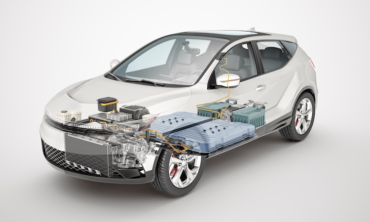
Image used courtesy of Adobe Stock
The OBC is used for AC charging and requires a single-phase or three-phase voltage from the grid. With one phase, the charging power is limited between 3.6kW and 7.5kW, with three phases 11 kW to 22 kW are supported. The market currently relies on OBCs in the medium power range (11 kW) as a compromise between cost and efficiency. 22kW is mainly used in the premium segment. However, every OBC must also support single-phase charging to be able to charge the vehicle even at limited power. Increasingly, OBCs are also required to be bi-directional to enable vehicle-to-grid (V2G) and vehicle-to-vehicle (V2V) charging solutions.
Until now, the design of OBCs has been based on standard discrete devices from the market, in THD or SMD. Especially with SMD components, challenges arise as heat needs to be extracted through the PCB or by carefully attaching each individual package with suitable thermal interface material to a heatsink. With this approach, the development towards higher power density and the associated system compactness is reaching its limits. Power modules are showing promising advantages for new product generations.
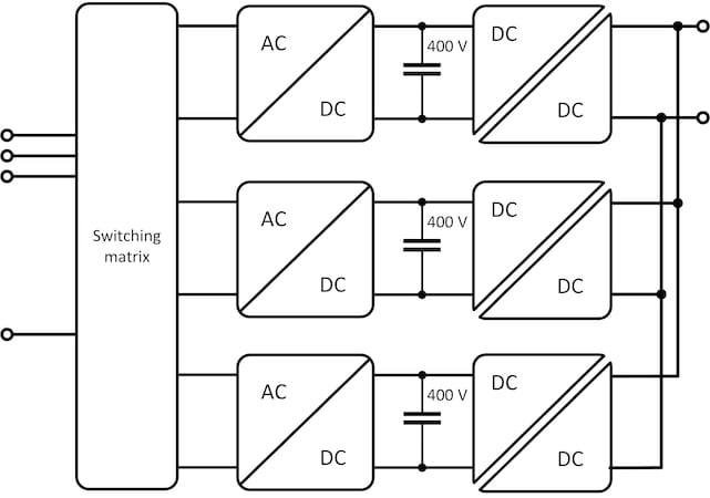
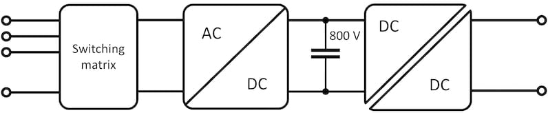
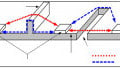
Figure 1. Modular (top) and centralized (bottom) architecture for OBCs. Image used courtesy of Bodo’s Power Systems [PDF]
Architecture and Topologies
There are basically two main architectures for OBCs (Figure 1): The modular architecture is based on three identical single-phase blocks. In contrast, the centralized architecture is based on a three-phase AC/DC converter, which is also capable of single-phase operation. Both architectures can be realized with unidirectional as well as bidirectional topologies.
The modular architecture requires more components and leads to higher overall DC link requirements in terms of stored energy content and thus volume and cost. Also, the modular architecture results in additional need for gate drivers and voltage / current sensing. In comparison, the centralized architecture allows for more cost-efficient OBCs, as fewer components are required. The centralized solution is the first choice for OBC solutions with high power density.
SiC Modules for Higher Efficiency and Power Density
Due to its excellent characteristics, SiC is ideally suited as material for power semiconductors in OBCs. Rohm’s 4th Generation SiC MOSFET based on a trench structure offers very low on-state resistance. In addition, the extremely low Miller capacitance enables very fast switching which leads to reduced switching losses. Together, this reduces the overall losses, which in turn leads to reduced constraints on the thermal dissipation.
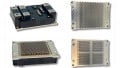
Rohm now extends the portfolio of SiC MOSFETs in the EcoSiC lineup with the new HSDIP20 modules, which are optimized for OBC applications. These modules integrate four or six SiC MOSFETs in a full bridge circuit. Compared to discrete components with the same chip technology, the modules offer several advantages.
The modules include Aluminum Nitride (AlN) ceramic to isolate the cooling pad from the drains of the MOSFETs. This results in a very low thermal resistance (Rth) between junction and case and eliminates the need for a TIM material that realizes electrical isolation between the cooling pad and the heatsink.
Thanks to the mold material, the various dies in the power module are electrically isolated from each other. This means that the chips can be placed much closer together than would be the case with discrete devices, where the creepage path on the PCB must be considered. This reduces the PCB footprint and increases the power density of the OBC solution.
Less Work at Less Risk
In addition to the technical advantages, the internal isolation facilitates the developer’s work: In the module, the functionality of the electrical insulation is handled within the module. For solutions with discrete components, the isolation needs to be externally addressed. The modules are tested by Rohm before delivery, so no further isolations tests are needed during the OBC development phase. The modules thus reduce time and development costs and at the same time reduce the risk of isolations issues.
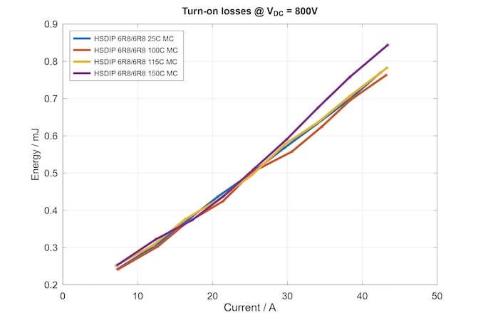
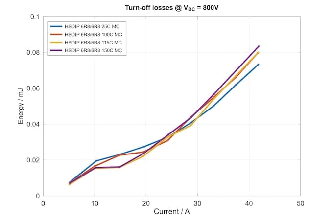
Figure 2. Turn-on and turn-off losses of the HSDIP Modules for different temperatures at a DC Link voltage of 800V. Image used courtesy of Bodo’s Power Systems [PDF]
Table 1. HSDIP20 power module lineup based on 4G SiC MOSFET. Image used courtesy of Bodo’s Power Systems [PDF]
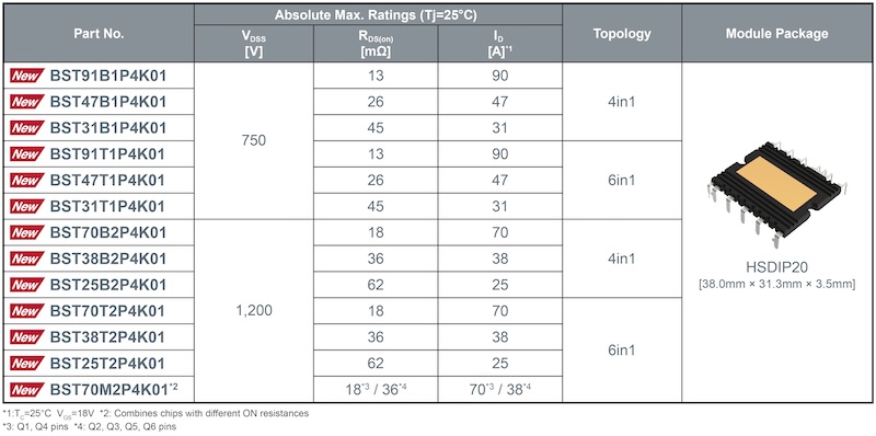
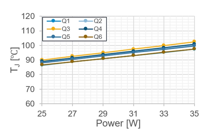
Figure 3. Simulation results of the thermal performance of the HSDIP modules. Image used courtesy of Bodo’s Power Systems [PDF]
The HSDIP20 modules also benefit from the additional advantages of the Gen 4 SiC MOSFETs: The 0V turn-off voltage reduces the complexity and costs of the PCB layout. As Figure 2 illustrates, the low switching losses of the Gen 4 SiC MOSFETs measured in HSDIP modules a DC link voltage of 800V for different temperatures.
Another advantage is the scalability: Rohm offers a broad lineup of RDS(on) values and topologies so that the modules can be used for different OBC power ranges. Six modules in 4-in-1-topology and six modules in 6-in-1-topology are available. In addition, a “hybrid” module in six-pack topology is available, which combines MOSFETs with different RDS(on) as a low-cost solution for totem pole PFC circuits to easily enable single-phase and three-phase operation with the same device. The modules are available in the same package regardless of the topology so that applications can be easily scaled. All power modules are qualified according to AQG324.
Thermal and Switching Characteristics
To illustrate the advantages of the HSDIP modules, the devices were characterized with simulations and measurements. The thermal performance of the modules is demonstrated using the sixpack module with 36mΩ, 1200V SiC MOSFETs. The simulation of a single module on a liquid cooled cold plate was carried out under the assumptions of 25 to 35W loss per chip, Ta=Tw=60 °C, TIM with a thickness of 20um and a thermal conductivity of 4.1W/mK. The power was injected simultaneously in the chips and then dissipated power vs. Tj of each device were plotted from the simulation (Figure 3).
With an optimized inner structure, the power module brings an advantage in thermal performances by keeping a very low thermal resistance per chip. The maximum junction temperature remains way below the 175 °C allowed for SiC MOSFETs, giving more room for increasing power density to address high power OBC requirements.
The switching loss behavior of the 6 in 1 module with 36mW, 1200V SiC MOSFETs was evaluated in a test board, that represents the AC/DC stage in an OBC application. The switching loss obtained in that measurement was already shown in Figure 2. The results of the evaluation of the switching losses by double pulse tests of this module also apply to the case of a bidirectional DC/AC stage considered here. Based on this data, a simulation of a bidirectional AC/DC stage for an 11 kW system was performed (Figure 4). The simulation results predict that an 11 kW AC/DC stage based on a 6 in 1 module with fourth generation SiC MOSFETs (36mΩ, 1200V) has an efficiency of about 99% at a switching frequency of 48 kHz and using a heat sink with forced air cooling. Only the semiconductor losses are considered.
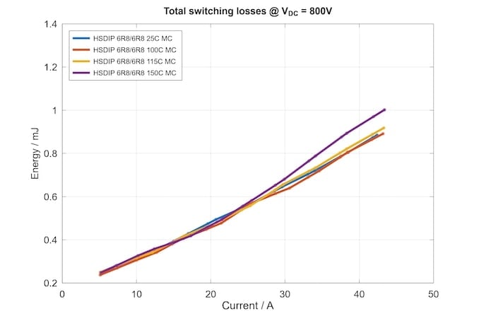
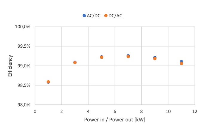
Figure 4. Simulation of the efficiency of the HSDIP modules in a bidirectional AC/DC stage of an OBC. Image used courtesy of Bodo’s Power Systems [PDF]
AC/DC stage for an 11 kW system was performed (Figure 4). The simulation results predict that an 11 kW AC/DC stage based on a 6 in 1 module with fourth generation SiC MOSFETs (36mΩ, 1200V) has an efficiency of about 99% at a switching frequency of 48 kHz and using a heat sink with forced air cooling. Only the semiconductor losses are considered.
Conclusion
Modules consisting of four or six SiC MOSFETs offer major advantages over individual devices when used in on-board chargers for electric and hybrid vehicles. Due to the higher power density, they enable a reduction in the size and weight of the OBC and lower the complexity of the design. Rohm’s HSDIP20 modules integrate the latest EcoSiC MOSFETs. In simulations, they show excellent thermal characteristics and 99% efficiency when used in the AC/DC stage of a bidirectional OBC.
References
[1] M. Jankovic, C. Felgemacher, K. Lenz, A. Mashaly and A. Charkaoui, “Cost and efficiency considerations in On-board Chargers,” 2022 24th European Conference on Power Electronics and Applications (EPE’22 ECCE Europe), Hanover, Germany, 2022, pp. P.1-P.9.
This article originally appeared in Bodo’s Power Systems [PDF] magazine and is co-authored by Imane Fouaide, Application Marketing Manager, and Christian Felgemacher, Senior Manager - Application Engineering, both Rohm Semiconductor.