Facebook
 Google
 GitHub
 Linkedin
Bipolar, Single Output, and Adjustable Power Supplies Based on the Common Buck Converter
This article shows how to use a buck converter to produce a bipolar PS when a dedicated bipolar supply IC is not an option.
A bench-top power supply (PS) tends to have an even number of terminals (ignoring the chassis port)—with one positive terminal and one negative terminal. Using a bench-top supply to produce a positive polarity output is easy: set the minus output to GND and the positive output voltage at the plus output. It is just as easy to produce a negative supply by reversing the setup. But what about producing a bipolar supply, where positive and negative voltages are both available to the load?
This is relatively easy, too—just connect the positive terminal of one lab channel to the negative of another channel and call that GND. The other two terminals, minus and plus, are the positive and negative supplies, respectively. The result is a three-terminal bipolar power supply with available GND, positive, and negative voltage levels. Because three terminals are used, there must be some switch between positive and negative supplies downstream of the power supply.
What if an application calls for the same power supply terminal to be positive or negative—a setup where only two terminals are provided to the load? This is not a purely academic question. There are applications in automotive and industrial environments that require bipolar, adjustable two terminal power supplies. For instance, two terminal bipolar power supplies are used in applications ranging from exotic window tinting to test and measurement equipment.
As noted earlier, a traditional bipolar PS produces two outputs using three output terminals: positive, negative, and GND. In contrast, a single output power supply should be equipped with only two output terminals: one GND and another that can be positive or negative. In such applications, the output voltage can be regulated relative to the GND by a single control signal, in the full range from the minimum negative to maximum positive. There are controllers that are specifically designed to implement the bipolar supply function, such as the LT8714, a bipolar output synchronous controller. Nevertheless, for many automotive and industrial manufacturers, testing and qualifying a specialized IC requires some investment in time and money. By contrast, many manufacturers already have prequalified step-down (buck) converters and controllers, as they are used in countless automotive and industrial applications. This article shows how to use a buck converter to produce a bipolar PS when a dedicated bipolar supply IC is not an option.
Circuit Description and Functionality
Figure 1 shows a buck converter-based solution for a bipolar (twoquadrant) adjustable power supply. The input voltage range is 12 V to 15 V; the output is any voltage in the ±10 V range, adjusted by the control block, that supports loads up to 6 A. The dual output step-down controller IC is the central component to this design. One output, connected per buck-boost topology, generates a stable –12 V (that is, the –12 V negative rail in Figure 1, with its power train comprising L2, Q2, Q3, and output filter CO2).
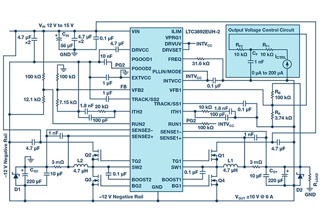
Figure 1: Electrical schematic of the two terminal, bipolar, adjustable power supply
The –12 V rail serves as ground for the second channel with the controller’s ground pins connected to the –12 V rail as well. Overall, this is a step-down buck converter, where the input voltage is the difference between –12 V and VIN. The output is adjustable and can be either positive or negative relative to GND. Note the output is always positive relative to the –12 V rail and includes a power train comprising L1, Q1, Q4, and CO1. The feedback resistor divider RB–RA sets the maximum output voltage. The value of this divider is adjusted by the output voltage control circuit, which can regulate the output down to the minimum output voltage (negative output) by injecting current into RA. The application start-up characteristics are set by the termination of the RUN and TRACK/SS pins.
Both outputs function in forced continuous conduction mode. In the output control circuit, the 0 µA to 200 µA current source, ICTRL, is connected to the negative rail as tested in the lab, but it can be referenced to the GND as well. The low-pass filter RF1–CF reduces fast output transients. To reduce the cost and size of the converter, output filters are formed using relatively inexpensive polarized capacitors. The optional diodes D1 and D2 prevent developing the reverse voltage across these capacitors, especially at startup. There is no need for the diodes if only ceramic capacitors are used.
Converter Testing and Evaluation
This solution was tested and evaluated based on the LTC3892 and evaluation kits DC1998A and DC2493A. The converter performed well in a number of tests, including line and load regulation, transient response, and output short. Figure 2 shows startup to a 6 A load, with a +10 V output. The linearity of the function between the control current and output voltage is shown in Figure 3. As control current increases from 0 µA to 200 µA, the output voltage decreases from +10 V to –10 V. Figure 4 shows the efficiency curves.
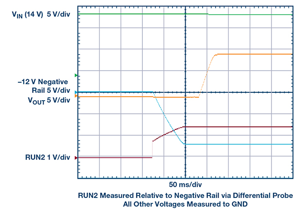
Figure 2: Start-up waveforms into resistive load.
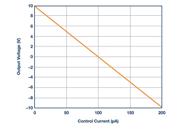
Figure 3: VOUT as a function of control current ICTRL. As ICTRL increases from 0 A to 200 µA, the output voltage drops from +10 V to –10 V.
An LTspice® model of the bipolar, two terminal power supply was developed to simplify adoption of this approach, allowing designers to analyze and simulate the circuit described above, introduce changes, view waveforms, and study component stress.
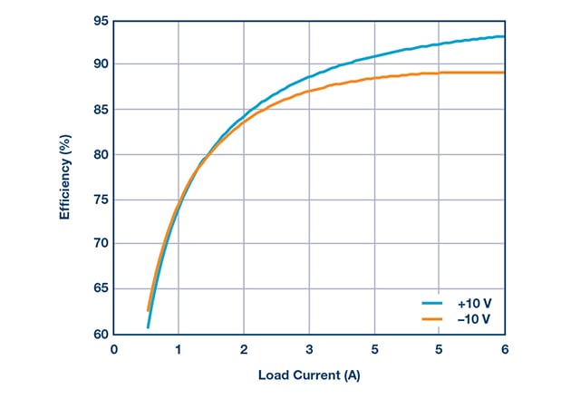
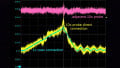
Figure 4: Efficiency curves for positive and negative output.
Essential Formulas and Expressions Describing this Topology
This approach is based on the negative rail, VNEG, generated by the buck-boost section of the design.
$$V_{NEG} = V_{OUT} + V_{OUT} \times K_m \ \ \ \ (1)$$
Where VOUT is the absolute value of maximum output voltage and Km is a coefficient ranging from 0.1 to 0.3. Km limits the minimum duty cycle of the step-down converter. VNEG also sets the minimum value of VIN:
$$V_{IN} \geq |V_{NEG}| \ \ \ \ (2)$$
$$V_{BUCK} = |V_{NEG}| + V_{IN}$$
Where VBUCK is the input voltage for the step-down section and thus presents the maximum voltage stress on the converter’s semiconductors:
$$V_{BUCK(MAX)} = |V_{NEG}| +V_{OUT} \ \ \ \ (3)$$
$$V_{BUCK(MIN)} = |V_{NEG}| - V_{OUT}$$
VBUCK(MAX) and VBUCK(MIN) are the maximum and minimum voltages of the step-down section of this topology, respectively. The maximum and minimum duty cycles and inductor current of the step-down section can be described by the following expressions, where IOUT is output current:
$$D_{BUCK(MAX)} = V_{BUCK(MAX)} / V_{BUCK} \ \ \ \ (4)$$
$$D_{BUCK(MIN)} = V_{BUCK(MIN)} / V_{BUCK}$$
$$I_{L(BUCK)} = I_{OUT} + \Delta I_I$$
The duty cycle of the buck-boost section of the PS:
$$D_{BB} = |V_{NEG}| / (V_{IN} + |V_{NEG}|) \ \ \ \ (5)$$
The input power of the step-down section and, correspondingly, output power of the buck-boost:
$$P_{OUT(BB)} = (V_{OUT} \times I_{OUT}) / \eta \ \ \ \ (6)$$
The converter power and input current.
$$I_{OUT(BB)} = P_{OUT(BB)} / |V_{NEG}| \ \ \ \ (7)$$
$$I_L(BB) = I_{OUT(BB)} / (1-D_{BB}) + \Delta I_2$$
The output voltage changes are executed by injecting current into the feedback resistor divider of the step-down section. Setting up the output voltage control is illustrated in the output voltage control circuit section of Figure 1.
If RB is given, then
$$P_{BB} = P_{OUT(BB)} / \eta \ \ \ \ (8)$$
$$I_{BB} = P_{BB} / V_{IN}$$
where VFB is the feedback pin voltage.
When the current source ICTRL injects zero current into RA, the output voltage of the buck converter is the maximum positive value (VBUCK(MAX)) relative to the negative rail and maximum output voltage (+ VOUT) relative to GND. To produce a negative output voltage to the load (relative to GND), the output voltage is reduced to its minimum value, VBUCK(MIN), relative to the negative output voltage (–VOUT), by injecting ΔI into resistor RA of the buck’s voltage divider.
Numerical Example
By using the previous equations, we can calculate voltage stress, current through the power train components, and the parameters of the control circuit for the bipolar power supply. For instance, the following calculations are for a supply generating ±10 V at 6 A from a 14 V input voltage.
If Km is 0.2, then VNEG = –12 V. Verifying conditions of minimum input voltage VIN ≥ | VNEG |. The voltage stress on the semiconductor’s VBUCK is 26 V.
The maximum voltage of the step-down section is VBUCK(MAX) = 22 V, relative to negative rail, setting the output voltage +10 V relative to GND. The minimum voltage, VBUCK(MIN) = 2 V, corresponds to the output voltage of –10 V relative to GND. These maximum and minimum voltages correspond to the maximum and minimum duty cycles, DBUCK(MAX) = 0.846, DBUCK(MIN) = 0.077, and DBB = 0.462.
Power can be calculated by assuming an efficiency of 90%, producing POUT(BB) = 66.67 W, IOUT(BB) = 5.56 A, IL(BB) = 10.37 A, and PBB = 74.074 W.
For an output voltage of +10 V (as per Figure 1), the control circuit current, ΔI, is 0 µA, whereas for an output voltage of –10 V, ΔI = 200 µA.
Conclusion
This article presents a design for bipolar, two-terminal power supplies. The approach discussed here is based on step-down converter topology, which is a staple of modern power electronics, and thus available in a variety of forms, from simple controllers with external components to complete modules. Employment of step-down topology gives the designer flexibility and an option to use prequalified parts, which saves time and cost.
About the Author
Victor Khasiev is a senior applications engineer at ADI. Victor has extensive experience in power electronics both in ac-to-dc and dc-to-dc conversion. He holds two patents and has written multiple articles. His patents are about efficient power factor correction solutions and advanced gate drivers. Victor enjoys supporting ADI customers: answering questions about ADI products, the design, and verification of power supplies schematics, and the layout of the print circuit boards; troubleshooting; and participating in testing final systems.
This article originally appeared in the Bodo’s Power Systems magazine.