Facebook
 Google
 GitHub
 Linkedin
Benchmarking Topologies for DC-to-DC Converters, the Heart of Off-Board Chargers
This article highlights Vincotech System Architectures and Topologies for DC-to-DC Converters that are the heart of off-board chargers.
Electrical vehicles (EVs) pose a host of questions, challenges and problems for people seeking to put this breed of car on the road. OEMs’ engineers have one set of issues to tackle, and infrastructure planners quite another, while policymakers are busy assembling the puzzle pieces of renewable energy, EVs and the smart grid. If we consider EVs in isolation, which is easily done on paper but difficult in the real world, the biggest issues are charging time and infrastructure availability.
These challenges will have to be mastered, for EVs are the future of transportation: As many as 120 million EVs could be up and running by 2030 [1], and the more EVs are on the road, the greater the collective fleet’s appetite for energy. Today charging energy demand amounts to around 20 billion kilowatt-hours, with forecasts calling for it to rise to 100 billion kilowatt-hours by 2025 and 280 billion kilowatt-hours by 2030 [1]. This is a tall order to fill – 2030 is just ten years down the road. More efficient EV chargers could help meet rising energy demands and deliver more power, faster. This article investigates various system architectures and topologies. It trains the spotlight on the DC-DC converters that are the heart of off-board chargers.
System Architectures
There are two main scenarios to ponder, public charging and home charging. Demand for each option varies by region. In view of China’s infrastructural constraints and densely populated cities, public charging is likely to be the far more frequent application in that country. In much of the USA, in contrast, home charging will dominate because so many people live in single-family houses. Then there is the nature of the charging device to contemplate – is it to be a slow charger, a fast charger or a high-power charger?

Figure 1: EV charger power levels
Batteries’ charging periods range from 20 minutes to 20 hours, depending on the output power of the electrical vehicle charger (EVC). Take, for example, an EV with 27.2 kWh net battery capacity. A 3-kW residential charger replenishes this battery’s capacity from 0% to 80% in nine hours. A DC-DC off-board fast charger (Level 3) does this in less than 45 minutes.
Figure 2: Average EV charging time
Three main system architectures were on the market at the time of writing. A quick review of each follows.
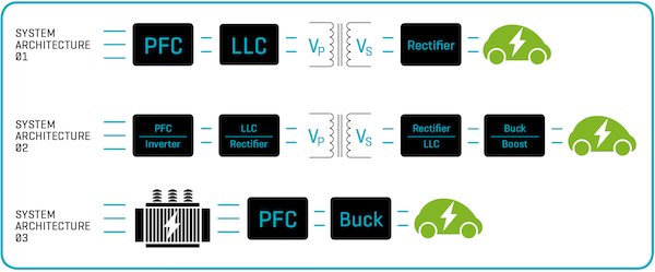
Figure 3: System architectures
System Architecture 1
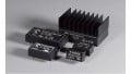
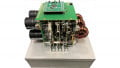
This is the state-of-the-art system architecture for up to 350 kW. Composed of several units, it is modular. The power level and type of power unit varies by regions. In China, for example, power units in the latest models of EV chargers are rated for 15 kW to 30 kW, and mainstream power units for 20 kW.
Most are based on telecom power supplies with discrete components that still satisfy today’s expectations for efficiency and reliability. Europe presents an entirely different picture, where even 20 kW power units are based on power modules to meet reliability and efficiency expectations and reduce manufacturing time. Much the same can be said of the USA.
System Architecture 2
This is a bidirectional vehicle-to-grid (V2G) system. It is designed mainly for residential applications where the EV serves as the storage unit. V2G is one of the key elements in smart-home applications and the smart grid. Again, it is just not feasible to consider EVs and EV chargers in isolation without factoring renewable energy and smart-grid penetration into the equation.
This is why system architecture 2 is gaining ground in applications ranging up to 22 kW and higher. Take, for example, a home-charging scenario where an American mother charges her compact EV at home, overnight. In this case, her car can actually serve as a buffer or energy storage unit for the household. This type of charger will make inroads into home-charging applications as the smart grid gains ground and renewable energy becomes a bigger factor in the energy mix.
System Architecture 3
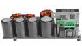
This latest design aims to serve the higher power (>200 kW) market. A medium-voltage transformer furnishes power directly to the system. There is a good reason why this has to be a medium-voltage transformer:
A highway-side charging station with ten chargers working at 350 kW each draws 3.5 MW from the grid. The power ought to be sourced from medium-voltage lines to meet this kind of demand. There are two ways of doing this. For one, we can use a conventional 50-Hz transformer to step the voltage down to 400 V (L-L) and then convert AC to DC. For the other, we can use power electronic transformer (PET) to generate medium-voltage, medium-frequency power with the power being converted within the transformer.
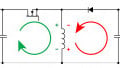
Used for years in traction applications, PET will be vital to the smart grid. DC-to-DC conversion is the heart of the system in all architectures. To date, the transformer has converted DC to DC to provide galvanic isolation between the car and mains power. The most frequently used topology is LLC. This is a zero-voltage-switching (ZVS) technique that serves to reduce switching losses, increase efficiency and energy density, and mitigate EMI issues. The next section briefly explains LLC topology and examines the results of an effort to benchmark component technologies’ cost and efficiency.
LLC Benchmark
A resonant LLC converter has advantages such as high efficiency, low EMI and increased power density. However, selecting the right component for the given application does require more effort.

Figure 4: Full-bridge LLC converter with a full-bridge rectifier
DC-DC conversion gain = turn ratio of transformers * resonant tank gain * switching bridge gain
where the gain of the full-bridge LLC is 1 [2].
A summary of the resonant LLC converter’s design parameters follows [2]:
- Quality factor (Q)
- Reflected road resistance
- Resonant frequency
- Ratio of primary inductance to resonant inductance (k)
The resonant LLC converter discussed in this paper was bench-marked using various component technologies at different resonant frequencies to rate efficiency and costs. The transformer’s conversion ratio is 1 and the maximum gain of the resonant tank is limited to 1.4. The Lr, Cr and Lm values depend on the transformer’s conversion ratio, the resonant frequency and the LLC’s designated power rating.
Several configurations with various component technologies are available. The double H-bridge consists of two cascaded H-bridges with 650 V components. The second configuration is an H-bridge with 1200 V components. The double H-bridge topology enables us to use 650 V components where the voltage at the PFC’s output is divided in two and routed to each H-bridge [3].
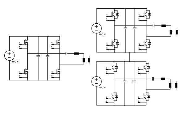
Figure 5: H-bridge topologies
| Chip set | 650V Fast IGBT - 100A |
| Topology | H-Bridge |
| Power | 12.5 kW |
| Vin | 400 V |
| Vout | 400 V |
| k factor | 9 |
| Q factor | 0.4 |
| Frequency range | 1-120 kHz |
| Chip set | 1200V Fast IGBT - 80A |
| Topology | H-Bridge |
| Power | 25 kW |
| Vin | 800 V |
| Vout | 800 V |
| k factor | 9 |
| Q factor | 0.4 |
| Frequency range | 1-120 kHz |
| Chip set | 650V Si-MOSFET - 20mOhm |
| Topology | H-Bridge |
| Power | 12.5 kW |
| Vin | 400 V |
| Vout | 400 V |
| k factor | 9 |
| Q factor | 0.4 |
| Frequency range | 1-120 kHz |
| Chip set | 1200V SiC-MOSFET - 20mOhm |
| Topology | H-Bridge |
| Power | 25 kW |
| Vin | 800 V |
| Vout | 800 V |
| k factor | 9 |
| Q factor | 0.4 |
| Frequency range | 1-120 kHz |
Fast IGBT and Si-MOSFET Solutions
The 1200 V SiC-MOSFET version exhibits the greatest efficiency throughout the frequency range. The 650 V Fast IGBT and 650 V Si-MOSFET solutions in double H-bridge topology exhibit similar performance beyond 100 kHz. The 650 V IGBT is more efficient at frequencies below 100 kHz.
However, the Si-MOSFET solution’s loss is lower than the IGBT solution’s at partial loads, which is attributable to the Rdson steepness. On the other hand, the 1200 V Fast IGBT’s performance dips drastically after 25 kHz. The cost benchmark provides a more complete picture. It clearly shows that the 1200 V SiC-MOSFET is the most expensive solution. The costs of the 650 V Fast IGBT and the 1200 V Fast IGBT are comparable and considered equal for the purpose of cost benchmarking. The Si-MOSFET, around twice as expensive as the Fast IGBT, falls midway between the two others in the cost ranking.
Note that this cost benchmark takes the power module’s price into account. This comparison assumes that the 1200 V SiC-MOSFET (single H-Bridge) comes in the Vincotech flow1 housing. The 650 V Fast-IGBT and 650 V Si-MOSFET are based on a double H-Bridge configuration, so they are taken to be housed in two Vincotech flow1 housings. Although the 1200 V Fast IGBT can come in a single module, this comparison assumes it is packaged in two Vincotech flow1 housings to distribute heat across two modules. The higher losses would otherwise make it impossible to disperse the heat from a single module. The trajectory of the efficiency curve at a partial load is a crucial issue. The graph below shows this partial load efficiency. Please note that the LLC is designed for a full load. Of course, this also determines its parameters.
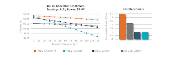
Figure 6: DC-DC converter benchmark under 25 kW full-load conditions
This benchmark for efficiency at partial load shows the 650 V Si-MOSFET outperforming the 650 V IGBT throughout the frequency range. This is explained by the lower power level – the reduced input current causes less static loss. Static losses generally outweigh switching losses in the LLC topology. Off-board DC-DC chargers supply the energy at full load to reduce charging time, which is why the comparison at full load is more meaningful.
The final question to be examined in this article is how much efficiency money can buy. We halved the 650 V Si-MOSFET’s Rds(on) to investigate how this affects efficiency. The graph below provides some answers.

Figure 7: DC-DC converter benchmark under 12 kW partial load conditions
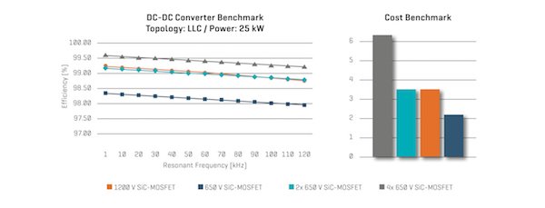
Figure 8: DC-DC converter benchmark under 25 kW full load conditions
As the above graph shows, paralleling 650 V Si-MOSFETs reduces losses and increases efficiency. If we halve Rds(on) to 10 mΩ, the efficiency level is on par with that of 1200 V SiC-MOSFET (20 mΩ). The next step is to reduce Rds(on) to 5 mΩ, which is done by paralleling the Si-MOSFET (20 mΩ). This again raises the system’s efficiency to a level beyond that of the SiC-MOSFET. As is to be expected, the modules’ price rises accordingly.
Note that doubling the 650 V Fast IGBT’s current rating would not increase efficiency as much as halving the Si-MOSFET’s Rds(on), which is why this option has not been explored. Conversely, doubling the Fast IGBT’s current rating does indeed reduce Rth, which helps cut losses by bringing the junction temperature down. This, in turn, enhances component reliability and extends service life.
Conclusion
This article briefly reviewed current EV chargers’ system architectures and zoomed in for a closer inspection of the LLC topology. The EV booming market has its challenges. As power levels increase, efficiency becomes an ever more important consideration.
The resonant LLC DC-DC converter is one of the most frequently used options in charger applications, but it is vital to select the right component and configuration for the application. The double-H bridge configuration with the 650 V Fast IGBT performs well in terms of both cost and efficiency.
The 1200 V SiC-MOSFET and 650 V SiC-MOSFET are good options if the application requires very high efficiency even at partial loads. Charging stations are a priority market for Vincotech. With its range of standard power modules and customer-specific solutions, the company offers the right solution to meet the demands of every customer’s applications.
About the Author
Baran Özbakır works as the Product Marketing Manager at Vincotech, Munich Area, Germany. He is responsible for the market analysis and marketing strategies for power supply industry; development of price strategies; product life-cycle management and cost calculation analysis and handling of technical and business requests for quotation. He is skilled in the field of power electronics, MatLab and electrical engineering. He earned his Bachelor's Degree in Electrical and Electronics Engineering at Yeditepe University located in Istanbul, Turkey. He then earned his Master of Engineering in Power Engineering at the Technical University of Munich located in Germany.
References and Notes
- Charging ahead: Electric-vehicle infrastructure demand by Hauke Engel, Russell Hensley, Stefan Knupfer, and Shivika Sahdev
- Application Note AN 2012-09 V1.0 September 2012 Resonant LLC Converter: Operation and Design 250W 33Vin 400Vout Design Example by Sam Abdel-Rahman
- Cost and Efficiency of Level-3 DC Fast-charging Power Modules—A Benchmark Comparison by Baran Özbakir
This article originally appeared in the Bodo’s Power Systems magazine.