Facebook
 Google
 GitHub
 Linkedin
Analyzing the Advantages of 100V GaN in 48V Applications
This article describes an ultra-low parasitics Eon/Eoff measurement platform and the advantages of 100V GaN in 48V applications.
In both consumer electronics and automotive electrification, we are in a cycle of “more” right now. For consumers, more videos, pictures, Insta-this, Snap-that are all driving data demands skyrocketing. In automotive, more features and functions are added to every model cycle including entertainment peripherals, safety features, hybrid motion torque, and additional and brighter LEDs. Providing “more” requires more power to be delivered. More power is typically constrained by size and/or weight restrictions. This is why a growing number of industries are moving to higher-voltage, 48V distribution versus conventional 12V distribution.
Why 48V? I2R conduction losses in a system can be detrimental to system efficiency and can reduce the power flow to the load effectively given cable, connector and/or PCB limitations. As an example, server processor power has increased from 100W-200W to 400W and higher. Distributing this increased power to multiple server processors creates more losses unless mitigated by higher voltage distribution or larger copper bus bars. The conventional datacenter/server power architecture is illustrated in Figure 1(a), where all major processor/ memory devices are powered from a 12V bus. The I2R loss for a 12V bus is excessive, and there are many energy conversion stages, which reduces the total system efficiency. To mitigate the heavy busbar loss and reduce energy conversion stages in the power distribution path, a 48V bus datacenter/server architecture is shown in Figure 1(b). This power architecture has an advantage over current design practices by eliminating online UPS, cables, and harness. The trend clearly shows that the power conversion benefits from 48V bus with more energy-saving and lower expenditure (CAPEX and OPEX).

a) Conventional power architecture with 12V bus

b) Alternative power architecture with 48V bus
Figure 1: The architecture evolution of datacenter/server from 12V to 48V
With “more power in less area” being the norm, moving from 12V to 48V power distribution using high-frequency power transistors allows engineers to meet their efficiency, cost and size/weight metrics.
The GaN Systems 100V product line is a solid solution candidate for 48V applications that meets high frequency, high efficiency, and high-power density power conversion requirements. Compared to MOSFETs, GaN transistors have a wide bandgap, high electron mobility, and high electron velocity to allow the system switching frequency to be pushed up to high kHz and MHz frequencies to maintain high efficiency and increase power density [1]-[4].
To optimize the system, a deep understanding of conduction and switching losses is required [5]. This information for higher voltage devices, e.g. 650V transistors, can usually be found in the datasheet as well as PLECS/Python simulation models provided by semiconductor companies. However, for 100V devices, the Eon/Eoff data is typically not published because of the difficulty of accurate measurement. An ultra-low parasitics Eon/Eoff measurement platform is described in this article. With this test platform, accurate Eon/Eoff data of 100V GaN Systems devices has been achieved.
GaN Systems provides the switching loss model including PLECS, Python and Excel-based for both 650V and 100V products. GaN Systems 100V GaN products, evaluation boards, modules, and the new set of PLECS simulation models provide a comprehensive place to start new system designs.
An Accurate Switching Energy Measurement Platform for 100V GaN Devices
When comparing transistors with different semiconductor materials, or analyzing trends from a specific manufacturer, the use of a standard figure of merit (FOM) is a useful tool. For example, to compare the RDS(on)*QG FOM of a 650V GaN Systems transistor versus a super junction MOSFET, there is more than a 10x difference in FOM and this has direct implications on system losses. Unlike 650V devices, the difference in FOM between GaN transistors from different suppliers and compared to silicon MOSFETs is not as large. The data below illustrates that additional understanding and measurement of device loss with accurate device loss models is required to determine the real system performance of the transistors in low voltage applications.
To measure the switch current during the switching transition process, a high bandwidth current shunt must be connected in series with the device under test (DUT). The parasitic inductance introduced by a large current shunt causes severe voltage overshoots when compared to the voltage rating of 100V devices. This results in the measured switching energy data being much higher than the value in real-world applications (without a current shunt used for measurement). As a result, power semiconductor vendors rarely publish switching energy data for 100V and below devices.
GaN Systems has designed an ultra-small parasitics Double-Pulse Test (DPT) platform, shown in Figure 2. The parasitic inductance of the power commutation loop is reduced from more than 10nH to 0.8nH, including the large current shunt (model #SSDN-005). When two adjacent conductors are located near each other with opposite current directions, the magnetic flux generated by the two directions of current will cancel each other, reducing the parasitic inductance.

Figure 2: Ultra-small parasitics DPT platform for 100V semiconductor devices


Figure 3: Comparison between the GaN Systems test platform (with Shunt) and other company evaluation board (without Shunt)
The distance between the two adjacent flux canceling layers of the DPT board is 62µm. The simulated power commutation loop inductance, according to ANSYS Q3D software, is 0.8 nH.
The comparison between the GaN Systems’ DPT platform and GaN transistor evaluation board for a different supplier, without a current shunt, is shown in Figure 3. Under the same test condition (Vds = 50V, Id = 10A, GaN device: GS61008T, Rg_on = 4.7Ω, Rg_off = 1Ω), the drain-source voltage spike on the DPT board is lower on GaN Systems design compared to the other design (68V versus 80V). This validates the flux canceling, low parasitics design of the GaN Systems test platform, even with a current shunt in circuit. Had a current shunt been used in the other design, the ringing would be significantly higher than 80V, and measuring Eon/Eoff would be highly inaccurate.


Figure 4: Eon/Eoff comparison between GaN Systems (GS61008T) and a silicon MOSFET
With the GaN Systems switching energy measurement platform, accurate Eon/Eoff data is achieved. A switching energy comparison between a GaN Systems device and a silicon MOSFET was achieved through testing. Both, the GaN transistor (GS61008T) and silicon MOSFET, have similar RDS(on). The results in Figure 4 show the GaN Systems device has lower Eon/Eoff than the silicon MOSFET.
Perhaps a more interesting comparison is between 100V GaN from different suppliers, as shown in Figure 5. Both GaN devices have similar RDS(on) values. However, the GaN Systems device has lower Eon/Eoff.
Figure of Merit
As described above, FOM is sometimes used to compare the incircuit performance capability of a given device technology in different applications. The following section shows how this can lead to incorrect conclusions with 100V device analysis.
In hard switching applications, two device parameters have major impact on the switching losses: 1) QGD, the miller charge, controls the voltage rising and falling speed; and 2) QGS, the gate source charge from the device threshold voltage to the gate plateau voltage, controls the current rising and falling speed. Therefore, the hard switching FOM = (QGD + QGS) * RDS(on) is usually used to compare the incircuit performance capability of different device technologies.


Figure 5: Eon/Eoff comparison between GaN Systems GaN (GS61008T) and other GaN with similar RDS(on)
In soft switching application, QOSS, the output charge, directly impacts the energy required to achieve zero voltage switching (ZVS) and zero current switching (ZCS). QG, which is the gate charge, is also a major switching loss characteristic in high-frequency soft switching applications. So, to compare parameters that influence the in-circuit performance of different device technologies in soft switching applications, FOM = (QOSS + QG) * RDS(on) is often used.
| GaN Systems GS61008T |
GaN Supplier 2 |
GaN Supplier 3 |
Silicon MOSFET |
|
| RDS(on) | 7 mΩ | 5.6 mΩ | 15 mΩ | 6 mΩ |
| QGS | 3.5 nC | 1.9 nC | 1.3 nC | 10 nC |
| QGD | 1.7 nC | 0.8 nC | 0.6 nC | 6 nC |
| QOSS | 21.3 nC | 25 nC | 21 nC | 41 nC |
| QG | 8 nC | 6 nC | 3.8 nC | 30 nC |
| Hard Switching FOM (QGS + QGD) * RDS(on) |
36.4 | 15.12 | 43.5 | 96 |
| Soft Switching FOM (QDSS + QG) * RDS(on) |
205.1 | 173.6 | 372 | 426 |
Table 1: FOM comparison of different semiconductor devices
A FOM comparison of four different semiconductor devices (three GaN transistors and one silicon MOSFET) is shown in Table 1.
According to the FOM comparison table, it can be observed that: 1) GaN devices have a lower FOM than silicon MOSFETs (remember that lower FOM is better); and 2) the product from GaN supplier 2 has the lowest FOM among the GaN devices. Interestingly, in this case, the device with the lowest FOM does not have the best performance in the targeted application. Recall from the Eon/Eoff analysis that the GaN Systems device has lower losses than the other GaN device. In addition to the Eon/Eoff losses, the thermal performance also contributes to overall functionality.
Thermal Performance and System-Level Comparison
In most applications, FOM and loss analysis is important but not the complete picture to achieve higher efficiency. Device thermal performance is also a very important factor to determine the system efficiency. GaN transistors have a positive temperature co-efficient RDS(on) characteristic. Also, switching losses increase as junction temperature increases. Therefore, devices with good FOM but difficulty managing thermal performance can have higher losses and be limited in efficiency and/or power.

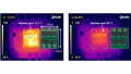
Figure 6: Thermal resistance comparison
As seen in Table 1, one GaN device has a better FOM compared to the GaN Systems device. However, there are some high power thermal challenges due to the “chip-scale” style package of the device. As shown in Figure 6, the GaN Systems device, in a low parasitic, thermally enhanced package, operates at ~50% lower TJUNCTION versus the chip-scale type device. To demonstrate the importance of thermals in an application, a system-level comparison is presented with the four different semiconductor devices from Table 1 used on identical 48V to 12V evaluation boards.
The maximum current versus switching frequency in Figure 7 shows that the GaN Systems’ device has 2.3x higher output power at 1MHz switching frequency compared to the other GaN devices and the silicon MOSFET.

Figure 7: Maximum current comparison vs. different switching frequency
The efficiency curve in Figure 8 shows that: • GaN transistors have much better efficiency over silicon MOSFETs; • the GaN Systems device has the highest efficiency; • the GaN Systems device can support much higher power compared to others.
Note that the tests were stopped when the specific device showed signs of thermals starting to limit output power. In this 48V to 12 V application, the data illustrates that a combination of FOM, Eon/Eoff and thermal performance must be considered to determine the best performance.

Figure 8: Efficiency comparison of different semiconductor solutions
Conclusion
GaN power transistors can switch at higher frequencies than traditional silicon MOSFETs and therefore are excellent power semiconductors candidates for 48V application challenges. System loss analysis is critical to optimize the power system design. To achieve accurate Eon/Eoff data for 100V GaN devices, GaN Systems has developed an ultra-low parasitics double-pulse test platform. The Eon/Eoff data acquired from this test platform shows that GaN transistors have lower Eon/Eoff than silicon MOSFETs and other GaN power devices. A system level comparison in a 48V to 12V application shows that 1) GaN Systems solutions achieve much higher efficiency than other GaN or silicon solutions, and 2) important factors such as Eon/Eoff loss analysis, packaging and thermal effects must be accounted for to achieve high system efficiency.
About the Authors
Lei Kou holds a PhD in Electrical and Computer Engineering at Queen's University, a Master's and Bachelor's Degree in Electrical Engineering at Hunan University. He has already achieved 9 publications throughout his career and is specializing in high-efficiency power converter design. Currently, he works as a Power Electronics Applications Engineer at GaN Systems Inc.
Juncheng (Lucas) Lu is the Applications Engineering Manager at GaN Systems.
References
- K. J. Chen, et al., "GaN-on-Si power technology: devices and applications," IEEE Transactions on Electron Devices, vol. 64, no. 3, pp. 779-795, Mar. 2017.
- F. C. Lee, Q. Li, Z. Liu, Y. Yang, C. Fei and M. Mu, "Application of GaN devices for 1 kW server power supply with integrated magnetics," in CPSS Transactions on Power Electronics and Applications, vol. 1, no. 1, pp. 3-12, Dec. 2016.
- J. Strydom, D, Reusch, "Design and evaluation of a 10 MHz gallium nitride based 42 V DC-DC converter," in IEEE 2014 Applied Power Electronics Conference and Exposition, 2014, pp. 1510-1516.
- D. Liu, Y. Wang, Z. Chen, and B. Li, "A buck converter with costeffective GaN/Si hybrid switches and CRM operation for high-efficiency and high-power-density applications," in IEEE 2018 Southern Power Electronics Conference, 2018, pp. 1-6.
- W. Chen, et al. "Impact of parasitic elements on power loss in GaN-based low-voltage and high current DC-DC buck converter," in IEEE 2018 International Conference on Electrical and Electronics Engineering, 2018, pp. 294-298.
This article originally appeared in the Bodo’s Power Systems magazine.