Facebook
 Google
 GitHub
 Linkedin
A Reverse Conducting IGCT Optimized for Medium Switching Frequency Applications
This article highlights ABB Semiconductors Reverse-Conducting Integrated Gate Commuted Thyristors platform or RC-IGCT in high power semiconductor device.
Highest Power Density for Most Compact Equipment
With the introduction of its latest Reverse-Conducting Integrated Gate Commuted Thyristors platform (RC-IGCT), ABB sets a new benchmark in high power semiconductor device performance. The initial RC-IGCT release is a 4500 V, 3600 A device. Available in variants optimized for medium switching frequency applications found with 3-level topologies, and for low switching frequency used in Multi-Level Modular Converters (MMC). The repetitive turn-OFF current of 3600 A is a record value in its class.
For the converter manufacturer, it means a significantly compact converter design than previously. The device can be used in many applications including medium voltage drive (MVD), power grid compensators, wind, rail-intertie and shore-to-ship.
Introduction
The advance in power conversion towards high power and high current, driven by renewable energy, grid stability and industrial drives, calls for compact power semiconductors with high current capability, low losses and high reliability. IGCT, compared to the ever-maturing IGBT technology, offers the following advantages:
- Low ON-state voltage, leading to lower total losses
- High current capability without paralleling
- Inherent ability to withstand large fault currents without rupturing
- Potential for stable short-circuit failure mode after failure
For this inverter type, the IGCT’s low loss advantage was quantified in [1]. Depending on the inverter mode, the losses are 10 – 15 percent lower using IGCTs than IGBTs.
This new IGCT platform is the culmination of some 20 years of continuous development.
Design
A key requirement is to retain the current outer dimensions for compatibility with the application and integrated gate unit.
The potential to expand the existing RC-IGCT platform offers:
- Increased device diameter through efficient use of raw silicon wafer.
- Minimal gate-circuit impedance – achieved by using a gate contact infrastructure at the device’s periphery and by routing the gate contact through the housing.
- Improved cooling by moving the gate contact to the periphery –now the pole piece trenches, used to convey the gate signal, are no longer needed.
- Increased maximum controllable current by adjusting the HPT+platform [2].
The device size has been increased from 91 to 94 mm, corresponding to 7 percent more area, by improving the respective capability of the manufacturing line.
By improving the thickness tolerance of the housing wall, a larger wafer diameter can be accommodated without changing the housing’s outer dimensions. As shown in Figure 1, by moving the gate contact radially outwards, its area consumption increases, provided other conditions remain the same. To counteract this effect, the device’s centering tolerance is lowered by more than 50 percent.
This results in a 21 percent increase in the active area available for performing the device’s function. The extra area is given entirely to the diode, whereas the IGCT area was made slightly smaller than the existing platform.

Figure 1: Left: The conventional RC-IGCT wafer with the gate contact in the separation between diode- and GCT parts. Right: The newly developed RC-IGCT wafer with the outer ring gate contact.
For turning OFF large currents, the IGCT is critically dependent on low gate-circuit stray impedance. The inductive impedance has three contributors: wafer, bushing and gate unit. The wafer and gate unit contributions are low in comparison to the bushing. With the new platform accommodating the peripheral gate, separation of gate and cathode can be decreased by routing the gate and cathode conductors close to each other, as shown in Figure 2.


Figure 2: Cross-sections of the gate-lead bushing of the earlier (left) and new (right) IGCT housing platform. The red parts show the current paths through the hermetic housing. ABB Switzerland Ltd is an owner of the design patents for both IGCT housing platforms
Silicon
Factors affecting the silicon design include resilience to cosmic ray induced failures, blocking capability and switching behavior, especially of the diode. The diode turn-OFF behavior at low currents and high voltages – the so-called snap-off behavior – governs the device’s thickness and resistivity.
Being fabricated on the same silicon wafer, the thickness and resistivity cannot be optimized separately for GCT- and diode parts. The device thickness is chosen to minimize the losses both in GCT- and diode parts, while maintaining diode snap-off and cosmic ray failure rate at an acceptable level [3].


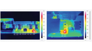
Figure 3: Thermal simulation output of the previous housing platform (left) and of the newly developed housing (right) at the same heating power density in the silicon wafer. Both GCT- and diode parts generating losses. The color indicates the temperature in °C, in the simulation. The maximal temperature of the new housing is 15 percent or 30°C lower.
Package
The new package design (without changing the outer dimensions of the housing) has eliminated some thermal bottlenecks compared to the previous version, as shown in Figure 3. Furthermore, the GCT- and diode parts are more connected, thermally, which can be used in applications where one part is more heavily loaded.
Optimization flexibility
Different lifetime tuning technologies enable diverse element optimization depending on the application’s needs, as shown in Figure 4. Increasing the ON-state voltage usually decreases the turn-OFF losses, shown in Figure 5. This gives the converter designer the flexibility to select the device best suited to the application (i.e. low or high switching frequency).


Figure 4: (Left) ON-state characteristics of the 4.5 kV device’s GCT part, showing the flexibility in tuning the IGCT for different switching frequencies (Fs). (Right) The corresponding ON-state characteristics for the diode part.


Figure 5: Trade-off between static and dynamic losses for both low Fs and high Fs variants of the 4.5 kV RC-IGCT. (Left) GCT part. (Right) diode part.
Device performance
The developed platform is subjected to the full range of reliability and electrical qualifications. In addition to repetitive validation of the device parameters, the robustness of the switch and diode is extraordinary, for the newly developed 4500 V/3600 A device variants. Figure 6 and Figure 7 show the current handling capability of a 4.5 kV device in single pulse turn-OFF measurements.


Figure 6: SOA waveforms of the 4.5 kV RC-IGCT’s GCT part at VDC = 3.2 kV. (Left) Tested up to 6.5 kA without failure at 25°C. (Right) The device controls current up to 5.5 kA at 135°C.

Figure 7: Demonstration of the 4.5 kV RC-IGCT for the diode part, recovering 4.5 kA against 3.9 kV DC at 135°C.
Conclusions
This paper highlights the latest developments for the Reverse-Conducting Integrated Gate Commutated Thyristors (RC-IGCTs) technology platform. The new platform offers a larger active device area and optimized gate contact design. This results in a higher controllable current over 6000 A in single pulse operation, improved diode conducting capability, and improved cooling.
The new technology platform further offers RC-IGCT variants, respectively optimized for medium and low switching frequency applications.The RC-IGCT 4500 V/ 3600 A, reported in this study, could be expanded to larger areas and higher voltage devices for any applications, including power grid applications based on MMC topology.
About the Authors
Umamaheswara Vemulapati worked as a Senior Scientist at ABB Switzerland Ltd. since October 2013. He was promoted and now works as the Principal Engineer since February 2019 at ABB located in Lenzburg, Switzerland.
Tobias Wikström works as a Project Manager at ABB Schweiz AG since July of the year, 2005, where he is responsible for the management of product development projects for bipolar power semiconductors and typical R&D projects including silicon; package, manufacturability, and electrical design; and reliability testing of products. He holds a Master's Degree in Material Physics from Uppsala University located in Sweden. He also has a Ph.D. in Electrical Engineering in which he earned at ET Zürich, a science, technology, engineering, and mathematics university in the city of Zürich, Switzerland.
Christian Winter works as the Global Product Manager of BiPolar Semiconductor Products at ABB Switzerland Ltd. – Semiconductors, Lenzburg, Switzerland. He is responsible as product manager for the BiPolar product portfolio consisting of the three lines: diodes, thyristors and IGCT / GTO, with production sites in Lenzburg and Prague. Developing, deciding and consolidating the product portfolio, the roadmap, the budgets of the corresponding development projects and the marketing strategies of the product lines. He earned his Höhere Technische Lehranstalt (HTL) in electrical engineering at the University of Applied Sciences and Arts Northwestern Switzerland or FHNW.
References
- Bjørn Ødegård, David Weiss, Tobias Wikström and Remo Baumann, “Rugged MMC converter cell for high power applications”, Proc. EPE 2016
- Martin Arnold, Tobias Wikström, Yoichi Otani, Thomas Stiasny, “High-Temperature Operation of HPT+IGCTs”, Proc. PCIM 2011
- Tobias Wikström, Maria Alexandrova, Vasilis Kappatos, Christian Winter, Evgeny Tsyplakov, Madhan Mohan and Makan Chen, “94 mm Reverse-Conducting IGCT for High Power and Low Losses Applications”, Proc. PCIM Asia 2017.
This article originally appeared in the Bodo’s Power Systems magazine.