Facebook
 Google
 GitHub
 Linkedin
Using MOSFET Controllers to Drive GaN EHEMTs
This article discusses the difference of Si MOSFET with separate controller driver, an integrated GaN/driver, and GaN power transistors with a separate controller drivers.
Before gallium nitride (GaN), the silicon (Si) MOSFET was the standard for power in adapter applications for decades. As a result, many of the existing controllers in the marketplace, including power factor correction (PFC) and DC-DC controllers, have already integrated silicon drivers into the controller chip. These controllers have proven to be a cost-effective and complete solution. However, the poor figure-of-merit (FOM) of Si MOSFETs limit the controller’s capability of high switching frequency performance to meet the requirement of high-power density vital to modern power systems.
GaN power transistors have demonstrated high-frequency performance advantages over Si MOSFETS for several years and continue to make significant advancements, including improving ease of driving the power transistor. Enhancement mode GaN (E-HEMTs) are driven with positive voltage between the gate and source, similar to N-chan-nel Si MOSFETs, provide a familiar solution for driving the devices. GaN Systems has a solution to easily use the MOSFET controller 12 V output voltage to drive the GaN 7 V gate input without the need of an external or integrated additional driver.
This paper describes an innovative circuit that permits the safe and reliable use of standard controller MOSFET drivers with GaN devices. The paper also compares this approach with an alternative of combining the driver and GaN power device into an integrated circuit.
GaN Technology Background and Drive Technology Requirements
GaN E-HEMTs eliminate the parasitic diode inherent in Si MOSFETs and have faster switching speeds and slew rates as well as higher operating temperatures that result from using a wide bandgap material. These and other improved characteristics allow GaN E-HEMTs to have reduced size and weight – a quarter that of a silicon design – and deliver lower system cost and increased efficiency as well.With their high-volume usage for Si MOSFETs, PFC and DC-DC controllers are widely available, and competition has made the pricing acceptable for even the most competitive Si MOSFET designs. However, as noted in the introduction, the output voltage of these devices is incompatible with the safe operating area (SOA) of e-mode GaN devices. Manufacturers of e-mode GaN devices have utilized a number of alternative drive schemes, all of which require alternatives to utilizing the standard Si MOSFET drivers.
An Integrated Circuit Solution
More recently, some manufacturers addressed this situation by developing a monolithic driving solution to allow use of Si MOSFET drivers. An integrated GaN/driver has the low drop out (LDO) regulator and driver integrated into a monolithic structure. The Si driving signal is regulated first, then drives the GaN using the GaN driver inside the chip. This approach actually has redundant drivers (external MOS-FET drivers and internal GaN drivers) that increase the cost and add complexity to the GaN devices.

Table 1: A high-level comparison of key characteristics of Si MOSFET with separate controller driver, an integrated GaN/driver, and GaN power transistors with a separate controller driver.

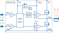
Figure 1: The EZ Drive solution consists of GaN transistors, a standard MOSFET controller, and discrete components.
An Easier Drive Solution
To avoid this cost and take advantage of readily available MOSFET controllers, GaN Systems developed a drive solution to utilize the Si driver inside the controller to directly drive the GaN E-HEMT. This topology is referred to as an EZDriveTM circuit. Table 1 shows a summary of advantages and disadvantages of the three driver designs.
A New GaN Design Tool: the EZDrive Solution
Figure 1 shows the diagram of the EZDrive solution for GaN E-HEMTs. It consists of a SI MOSFET controller with drivers integrated, a small number of external components (two resistors, two capacitors, two sets of back-to-back Zener diodes and one general diode), and discrete GaN E-HEMTs.

Figure 2: With operation modes similar to a conventional non-isolated bootstrap high side/low side driver, the EZDrive circuitry allows a wide (9~18 V) controller driving voltage range.

Figure 3: Verification measurements in the LLC stage demonstrate exceptional performance of the EZDrive circuit.
Transistor |
PFC/LLC Controller |
External Driver |
Integrated Driver in FETs |
Multisource Devices |
Transistor Range |
Silicon MOSFET |
Several available from ON Semi, TI, STMicro and others. Examples include:
|
NO
|
NO
|
YES
|
Widest |
Monolithic-Integrated GaN |
NO
|
YES
|
NO
|
Narrow |
|
GaN Systems |
NO
|
NO
|
YES
|
25, 50, 67, 100, 150,
|
Table 2: The summary of the advantages and disadvantages of the three drivers discussed in this article.
EZDrive solution three operating modes
The EZDrive solution has three operating modes which are similar to those of the conventional bootstrap half-bridge driver. As shown in Figure 2, in Mode 1, assuming the Vcc of the controller is 12 V, the high-side GaN is OFF and the low-side GaN is ON. The driving voltage on the low-side GaN is clamped at 6 V by the Zener diode and the rest of the Vcc (6 V) is stored across the capacitor CUD2. In this mode, CBoot is charged.
In Mode 2, both the high-side and low-side GaN devices are OFF. The voltage stored in CUD2 is applied to the gate reversely, so the low-side GaN can be turned OFF quickly. In this mode, CBoot is still charged.
Finally, in Mode 3, the high-side GaN is ON and the low-side GaN is OFF. Cboot is discharged providing the driving voltage to the high-side GaN.
In comparison with an integrated GaN/driver approach, the number of external components is similar with the EZDrive solution requiring 11 components (turn ON/OFF gate resistors included), while the monolithic approach requires 10. However, the integrated GaN/driver suffers from high cost and complexity because of the redundant GaN driver and LDO regulator in the chip.
Since the driver and gate are connected inside the chip in the monolithic approach, the gate resistor is not adjustable. This makes the current, charging and discharging the gate, a fixed value that influences (fixes) the switching speed of the power device and limits the ability to address electromagnetic interference (EMI) and other gate drive aspects.
EZDrive Solution Verified in Different Circuits
To verify the EZDrive performance, a half-bridge GaN daughter card was designed with EZDrive external components on it. This circuitry was applied to an LLC stage with Si MOSFETs replaced by the daughter card: Vcc=12 V, Vin = 400 V, Vout = 12 V and the LLC controller is the NCP13992. The driving voltage is 6.5 V/-5.8 V. Measurement results are shown in Figure 3.
The experimental results show that no overshoot/undershoot occurs on the driving voltage or VDS under all operating conditions. In addition, the operating temperature is quite low with maximum temperatures below 44°C (well below the safe maximum operating temperature).
The EZDrive solution has also been applied to a PFC stage. To do this, a daughter card was used with diode, GaN transistors, the EZDrive circuit, and a current sensing resistor. As a result of this effort, suggestions on layout to reduce the trace inductance as well as the mutual inductance have been developed.
Even Easier
To make designing with GaN power transistors even easier, evaluation kits with the EZDrive circuit are available. As shown in Figure 4, with the EZDrive circuit, GS-065 low current 3.5 A, 8 A, and 11 A evaluation kits provide a low-cost, easy to implement solution that offers greater design flexibility and reduces the number of system components. In addition to the evaluation kits, reference designs and circuit simulation tools from GaN Systems and its ecosystem partners enable design engineers to take advantage of the benefits of GaN power transistors – high efficiency and low size, weight, and total system cost – with even quicker time-to-market.
Taking Full Advantage of GaN Technology
All of the proven advantages of GaN technology over Si MOSFETs can be realized with the right controller design. Driving GaN transistors directly with existing high-volume MOSFET controllers simplifies GaN designs and reduces the cost of implementing the drive circuit. In addition, using discrete GaN transistors provide customers a wide range of products and multiple sources of GaN devices.
The EZDrive solution converts any IC controller/driver to properly drive GaN Systems E-HEMTs. This eliminates the redundant GaN drivers and LDOs in a monolithic, integrated driver GaN device or as discretes reducing size and cost. In addition, the turn ON/OFF slew rate is controllable with external resistors for complete control of EMI. The EZDrive solutions apply to single, dual, or half-bridge controllers with Si MOSFET drivers.
EZDriveTM is a trademark of GaN Systems, Inc.

Figure 4: GaN Systems’ EZDrive Evaluation Board, the GS65011L-EVBEZ.
About the Authors
Yajie Qiu is the Senior Power Electronics Applications Engineer at GaN Systems.
Juncheng (Lucas) Lu is the Applications Engineering Manager at GaN Systems. GaN Systems is the global leader in GaN power semiconductors with the largest portfolio of transistors that uniquely address the needs of today's most demanding industries including data center servers, renewable energy systems, automotive, industrial motors and consumer electronics.
This article originally appeared in the Bodo’s Power Systems magazine.