Facebook
 Google
 GitHub
 Linkedin
GaN ePower Integrated Circuits Applied to Motor Drives
The latest ePower™ integrated circuits based on gallium nitride technology by Efficient Power Conversion are revolutionizing motor drive applications such as industrial drones, e-bikes, scooters, and power tools.
Since its introduction, gallium nitride technology has opened a new era in the world of power electronics. The main differences between gallium nitride and silicon technologies are well described in [1] and are summarized in Table 1.
| Parameter | Silicon | GaN | |
| Band Gap Eg | eV | 1.12 | 3.39 |
| Critical Field Ecrit | MV/cm | 0.23 | 3.3 |
| Electron Mobility µn | cm2/V•s | 1400 | 1500 |
Table 1. Material properties of GaN and Si.
The three most important parameters in this comparison are the higher bandgap, critical field, and electron mobility. The critical field, measured in volts per centimeter, determines the threshold for avalanche breakdown. The voltage at which a device breaks down is therefore proportional to the width of the drift region. In the case of GaN, the drift region can be 10 times smaller than in silicon for the same breakdown voltage. When these parameters are all combined, if the critical field of the crystal is 10 times higher, it follows that the electrical terminals can be 10 times closer together. This leads to a clear differentiation factor between GaN and silicon: medium voltage gallium nitride devices can be built on a planar technology while this is cost-prohibitive for silicon devices. To be competitive, silicon devices are made on a vertical technology, usually with gate and source on the top and drain on the bottom, making it physically impossible to have two power devices in the same chip. EPC’s GaN-on-Si planar technology does not have this limit of having to be built vertically, and a schematic cross section of an integrated circuit that takes advantage of this is shown in Figure 1.

Figure 1. EPC gallium nitride technology enables integration of power devices with gate driver logic. Image used courtesy of Bodo’s Power Systems
Starting with discrete lateral eGaN® FET devices, EPC quickly moved to higher levels of integration. In 2014, EPC introduced a family of integrated devices comprised of multiple FETs on one chip, which became the starting point for the journey toward a power systemon-a-chip. This trend was expanded with the introduction of the EPC2107 and EPC2108, integrated half bridges with integrated synchronous bootstrap transistors.
In 2018, EPC continued on its integration path with the introduction of GaN ICs combining gate drivers with high-frequency GaN FETs in a single chip for improved efficiency, reduced size, and lower cost. In 2019, the ePower Stage IC family of products redefined power conversion by integrating all requisite power system-on-a-chip functions in a single GaN-on-Si integrated circuit at higher voltages and higher frequency levels - beyond the reach of silicon. Most recently, in 2021 the EPC23101 in combination with the EPC2302 power stage chipset was introduced to the market.
GaN Integrated Circuit Monolithic Power Stage – EPC2152
The first ePower Stage device was introduced in 2019. The EPC2152 is a monolithically integrated single-chip driver plus GaN FET half bridge power stage IC. Input logic interface, level shifting, bootstrap charging, and gate drive buffer circuits, along with GaN output FETs configured as a half bridge, are integrated within a monolithic chip. This integration resulted in a chip-scale LGA form factor that measures only 3.85 mm x 2.59 mm x 0.63 mm. The two GaN output FETs in half-bridge topology are designed to have the same 8.5 mΩ typical RDS(on).
Integration of GaN FETs with on-chip gate drive buffers practically eliminates the effects of common source inductance and gate drive loop inductance. Power loop inductance is minimized by the LGA pinouts that facilitate the internal vertical layout technique. The block diagram of EPC2152 is shown in Figure 2 and the reference design, EPC9146 BLDC inverter functional block diagram is given in Figure 3.

Figure 2. EPC2152 GaN integrated circuit block diagram. Image used courtesy of Bodo’s Power Systems

Figure 3. EPC9146 BLDC inverter functional block diagram. Image used courtesy of Bodo’s Power Systems
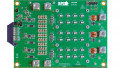
EPC9146 Motor Drive Reference Design with EPC2152
To demonstrate the capabilities of the EPC2152 integrated circuit in a motor drive inverter, EPC released the EPC9146 reference design. It is a three-phase brushless (BLDC) motor drive inverter board that contains three EPC2152 monolithic ePower stages, 15 Apk (10.5 ARMS) maximum output current. Besides the monolithic power stage, the board contains all the necessary critical functions to support a complete motor drive inverter, including regulated auxiliary power rails for housekeeping supplies, voltage, and temperature sensing, phase current sensing, and protection functions. The various functional blocks of the EPC9146 are shown in Figure 3. This reference design can be used for all applications where the motor phase current is 10 ARMS continuous with 15 ARMS high current operation for a limited time.
GaN IC Power Stage Chipset – EPC23101 in Combination with EPC2302
Following the path toward further integration and increased power density, in 2021 EPC introduced a chipset combining the EPC23101, a high-side GaN with a monolithically integrated Half-bridge gate driver, and the EPC2302 GaN FET, as depicted in Figure 4.
The EPC23101 is a 100 V rated monolithic component that integrates input logic interface, level shifting, bootstrap charging, and gate drive buffer circuits, along with a high-side, 2.6 mΩ typical RDS(on) GaN output FET. The EPC2302 is the 100 V companion lowside, 1.4 mΩ typical RDS(on) GaN FET. Over-voltage spikes can be controlled to less than +10 V above the rail and –10 V below ground during hard switching transitions by choosing the tuning resistors, RBOOT and RDRV.
The EPC23101 IC requires only an external 5 V (VDRV) power supply. Internal low-side and high-side power supplies, VDD and VBOOT, are generated from the external supply via a series-connected switch and a synchronous bootstrap switch. The internal circuits can be disabled to reduce quiescent power consumption by connecting the EN pin to VDRV. The FET gate drive voltages are derived from the internal low side and high side power supplies. Full gate drive voltages are only available after the HSIN and LSIN PWM inputs operate for a few cycles. Compared to the EPC2152, the EPC23101 in combination with the EPC2302 allows designers to make higher current inverters.

Figure 4. EPC23101 in combination with EPC2302 GaN IC chipset block diagram. Image used courtesy of Bodo’s Power Systems
EPC9173 Motor Drive Reference Design with EPC23101
To demonstrate the capabilities of the EPC23101 IC in a motor drive inverter, EPC released the EPC9173 reference design. On this board, each half bridge of the three-phase inverter comprises two EPC23101 ICs with their PWM signals cross-connected allowing the insertion of a source shunt to read the current, and shown in Figure 5, with a portion of the schematic.
By using the same IC for the low-side switch, it is possible to have a balanced half-bridge inverter and both switches can float with respect to the Power Ground. This makes the insertion of the source shunt easier, avoiding ground bouncing on the input PWM signal nodes. The EPC9173 board includes an over-current detection circuit that can be used either as an over-current or as a current-limit function, depending on the desired algorithm and modulation.

Figure 5. EPC9173 BLDC inverter functional block diagram. Image used courtesy of Bodo’s Power Systems
Applications
PWM frequency increase and dead time reduction
GaN integrated circuits and FETs bring several advantages in motor drive applications. The easiest advantage to understand is the reduction of inverter size, which is due to an intrinsic smaller dimension of a GaN FET and ICs versus the equivalent MOSFET. However, to get the most out of the new technology, it is better to operate a motor at a higher PWM frequency and to consequently reduce the dead time [2].
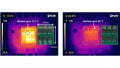
Conventional silicon MOSFET inverters are constrained by high switching losses and by the commutation behavior, and usually are not operated above 40 kHz PWM frequency and with dead time lower than 200 ns. GaN-based inverters are not limited in this sense and can increase the efficiency of the motor because of lower ohmic dissipation due to reduced current ripple (Figure 6, [4]) and fewer torque harmonics that are responsible for motor vibrations [2].

Figure 6. Comparison between measured and estimated PWM-induced losses in a motor with 50% duty cycle square wave voltage excitation [4]. Image used courtesy of Bodo’s Power Systems
Moreover, increasing switching frequency helps to reduce the input filter and to remove the need for electrolytic capacitors. A comparison between two inverters, one running at 20 kHz, 500 ns dead time, and the other, based on GaN, running at 100 kHz, 14 ns dead time is shown in Table 2. The GaN inverter has no input inductor and uses only two ceramic capacitors. Both inverters were operating in the same setup in the same conditions, and the motor is more efficient because many energy wasting harmonics were removed in the GaN inverter case.
Applications with Low L/R Time Constant in the Motor
All applications that require high electrical frequency and fast dynamics, such as drone propellers and e-bike in-pedal motors, use very low inductance (single-digit ΩH range) motors. With the advent of more efficient magnetic circuit designs realized by better materials and higher strength permanent magnets, the number of turns on an electromagnetic phase can be reduced and still produce the same back-emf.
| Setup | Inverter 20kHz, 500 ns dead time 400 RPM, 5 ARMS | GaN inverter 100 kHz, 14 ns dead time 400 RPM, 5 ARMS |
| Input Inductance | 2.7 µH | None |
| Input Capacitor | 660 µF electrolytic | 44 µF ceramic |
| Pin | 121.3 W | 113.3 W |
| Pout | 119.6 W | 113.3 W |
| ninverter | 98.50% | 98.20% |
| Speed | 42.25 rad/s | 41.94 rad/s |
| Torque | 1.876 Nm | 1.940 Nm |
| Pmech | 79.3 W | 81.36 W |
| nmotor | 66.30% | 73.10% |
| n total efficiency | 65.30% | 71.80% |
Table 2. Comparison between 20 kHz, 500 ns inverter and 100 kHz, 14 ns GaN inverter with reduced input filter [2].
Permanent magnet brushless motors generate back-emf voltage, e, proportional to speed, ω (e = Ke·ω), and the maximum speed a given motor can run is directly related to the DC bus voltage and the voltage constant, Ke. To increase the speed, it is necessary to lower Ke, by reducing the phase coil turns count, which reduces the inductance by the square of the difference. Limiting the current ripple to less than 10% of the phase current is a good design practice and can be only achieved by increasing the PWM frequency.
The current rise with time is related to the ratio of voltage to inductance, and as inductance decreases, the current rises quicker, as does the PWM induced current ripple. The decreased current rise time and larger ripple increases the amount of heat generated and creates additional EMI noise, which is not desirable. In general, these motors have a small time-constant, \(\tau=\frac{L}{R}\), that can benefit from a 100 kHz PWM frequency.
Input Current and Voltage Ripple
The input voltage ripple ∆vin in an inverter is proportional to the output phase current and inversely proportional to the PWM frequency and input capacitance, as per eq. (1)
\(\Delta v_{in} \infty\frac{1}{f\,P\,W\,M\,}\frac{1_{phase}}{C_{in}}\) (1)
The desired ripple depends on the EMI constraint given by the emissions generated by the cables from the dc source to the inverter. If the PWM frequency is in the range of 20 kHz, the required input capacitance Cin can only be practically obtained by using electrolytic capacitors that are bulky and less reliable than ceramic capacitors.
Moreover, the electrolytic capacitors are limited by the RMS current that can flow through them, thus requiring more capacitors in parallel and resulting in a total input capacitance that is higher by more than one order of magnitude than needed for a design. When the frequency is increased to 100 kHz, designers can use ceramic capacitors such as X7R, keeping in mind, as a design rule, the effective capacitance drops to half of the specified value when the applied voltage is half of the rated voltage.
The EPC9173 reference design provides for both electrolytic and ceramic capacitors, giving chance for designers to select their preferred switching frequency and to add or remove the capacitors as preferred.
Power Tools with Trapezoidal Modulation
Many power tools applications are still using trapezoidal modulation schemes and related inverter schematics. Usually, these applications are based on three hall sensors to detect the rotor position with a resolution of 60 electrical degrees, and they have a single shunt to measure the current in the DC bus return. The six-step operation has many advantages for BLDC drives, such as maximum power utilization and widened flux-weakening region.
However, due to the maximum utilization of inverter output, a saturation of the current regulator makes it difficult to maintain instantaneous current control capability. In most conventional systems it is implemented by voltage angle control with cycle-by-cycle current limit, with unsatisfactory dynamic performance. If the current limit is reached during the PWM cycle, the energizing device (depending on the current direction) is switched off until the next PWM cycle.
The principle of the BLDC motor is to energize the phase pair, which can produce the highest torque. To optimize this effect the back-emf shape is designed to be trapezoidal, but, in reality, it is sinusoidal with some higher harmonics. The combination of a DC current with a trapezoidal back-emf makes it theoretically possible to produce a constant torque. In practice, the current cannot be established instantaneously in a motor phase. As a consequence, the torque ripple is present at each 60-degree phase commutation.
With the current-limiting cycle-by-cycle scheme and low inductance motors, the lower the PWM frequency, the higher the current ripple. This in turn generates heat and unnecessary power dissipation. Using a GaN inverter, with the same trapezoidal scheme, makes it possible to increase the PWM frequency and then reduce the current ripple, obtaining higher efficiency, less heat, and fewer vibrations.
The GaN motor drive reference designs EPC9173 and EPC9167 are equipped with a current comparator circuit whose output can be used by the microcontroller as a signal for cycle-by-cycle current limiting to follow a trapezoidal modulation. With this system, power tools designers can test the reference designs to assess the GaN advantage in their application.
Conclusions
When dealing with motor applications, GaN inverters can increase the efficiency of the system if PWM frequency is increased, the dead time is drastically reduced, and the input capacitance is converted from electrolytic capacitors to ceramic capacitors. Using EPC’s new GaN integrated circuits, such as the EPC2152 and EPC23101, results in increased power density and system efficiency, while saving much system design effort.
This article originally appeared in Bodo’s Power Systems magazine.
Related Content