Facebook
 Google
 GitHub
 Linkedin
More Power and Higher Reliability by 7th Generation IGBT Module with New SLC Technology
This article highlights Mitsubishi Electric Corporation SLC package technology is combined with the 7th Gen Chip in the NX-type IGBT Modules Series.
The main requirements of power electronics system are high efficiency, high power density, and high reliability. To achieve high efficiency, Mitsubishi Electric developed the 7th Gen IGBT chipset. To additionally fulfill the requirements of high reliability and high power density, the newly developed SLC package technology is combined with the 7th Gen Chip in the NX-type IGBT Modules Series.
Industrial IGBT Modules are used in various fields of applications. All those applications require compact power modules with high power density, high reliability and high efficiency with reasonable cost.
To fulfill all these requirements, the 7th Gen NX-type IGBT Modules based on SLC-Technology have been developed. The 7th Gen IGBT, which is based on CSTBTTM (Carrier Stored Trench Gate Bipolar Transistor) concept, provides high efficiency by the reduction of dynamic and static losses [2].
The loss reduction is the first step to realize a high power density module. In a second step, the thermal resistance Rth must be improved in order to increase the power capability at a given operating temperature and to reduce the temperature swings. By combining improved temperature and power cycling capability, high reliability and compact power modules can be realized. The newly developed SLC-package technology provides low thermal resistance and high power and thermal cycling capability.
What is SLC Technology?
SLC (SoLid Cover) Technology is a newly developed package technology for realizing high reliability and high thermal conductivity [3]. The comparison of the new package structure with a conventional structure is shown in Figure 1.
Metalized ceramic substrates are conventionally used to realize the electrical insulation between the electrical circuit with semiconductor chips and the module’s base plate. Those substrates are joined to the copper base plate by a solder layer. The disadvantage of this material combination is the mismatch of CTE (Coefficient of Thermal Expansion) between ceramics, solder, and copper. This mismatch causes solder cracks by temperature swings and limits the longevity of power modules. The module’s withstand capability against this stress is known as temperature cycling capability.
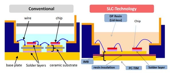
Figure 1: Comparison of SLC and conventional package structures
In SLC technology, the insulation is made of a resin material which has a similar CTE value as copper. The base plate and the solder layer are eliminated because the top and bottom side copper layers can be directly bonded to the insulating resin layer. By this IMB (Insulated Metal Baseplate) the thermal cycling capability is essentially improved. Current status of the ongoing temperature cycle test is shown in Figure 2.
Currently, it has reached 40K cycles at 80K temperature swings. This result is about 7 times higher than the conventional capability, and this test is still ongoing without failure. Furthermore, as shown on the right side of Figure 2, after 40K cycles, no delamination at all could be observed so far. Therefore, even higher thermal cycling capability is expected.
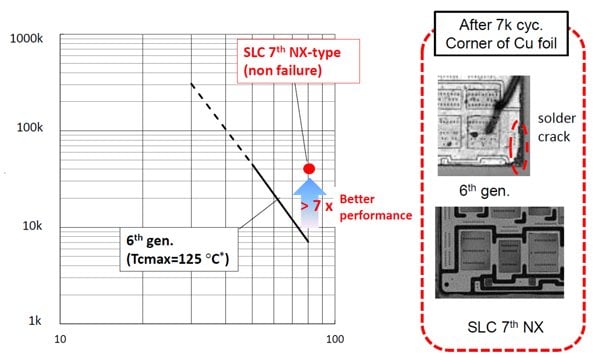
Figure 2: Thermal cycle test status
Thermal Cycling Capabilities with SLC Technology
In conventional modules, the maximum size of those ceramic substrates is limited to the thermal cycling capability because the mechanical stress applied to the solder layer caused by temperature swings is increasing with larger substrate size. Therefore in conventional IGBT Modules with a base plate size of 122mm x 62mm usually two or three ceramic substrates are used as shown in Figure 3.
On the other hand, the new SLC-technology consists of one common IMB owing to the elimination of the solder layer between substrate and baseplate. By this common substrate approach, the effective area available for mounting power chips in the module is expanded and wire bond connections between the substrates are eliminated, thus reducing the internal parasitic package inductance and also the lead resistance. Hence, the common IMB is one key element of the SLC-technology to achieve compact power modules with high power density.
Power Cycling Capabilities with SLC Technology
Besides the thermal cycling capability, also the power cycling capability must be considered to develop a high-reliability power module. The main root cause of the power cycling failure mode is the degradation of the bonded wires joint. Continuously current flow and the related junction temperature swings cause strain at wire bonds.
In the new SLC technology, the bond wires are covered by hard direct potting resin instead of soft silicone gel. By this hard DP-Resin, the mechanical stress of the wire bond is spread homogeneously to the whole surface of the wire as shown in Figure 4. In a conventional power module, the mechanical stress of the wire is not absorbed so much by the soft silicone gel and that stress is concentrated to the base of the bonding wire.
The 6th Gen. IGBT modules already apply an optimized and improved wire bonding technology to achieve the high power cycling lifetime with aluminum wires and soft silicone gel coat. Moreover by the combination of this wire bonding technology and the SLC technology, the power cycling capability is essentially improved by keeping the well-approved aluminum wire bonds with their known cost advantages compared to expensive technologies like copper wire bonding. The comparison between the target power cycling capability of the SLC-technology and the 6th Gen. modules is shown in Figure 5.

Figure 3: NX-type package with 1 IMB and 2. Conventional ceramic substrate

Figure 4: Stress concentration to the wire bond with Conventional and SLC-Technology

Figure 5: Power cycling capability of Conventional and SLC Technology
To have a further improvement of the power cycling lifetime, the junction temperature swing should be reduced. This can be achieved by improving the thermal resistance of the power module. Applications with constant load are usually thermally limited by the maximum junction temperature specification.
SLC-technology has improved thermal resistance
To cover also these requirements, the SLC-technology has improved thermal resistance. SLC-technology applies the IMB, therefore the solder layer which has a low thermal conductivity between substrate and baseplate is eliminated. The insulation material and the thickness of the insulation layer of the IMB are selected to achieve the best trade-off of insulation capability, reliability, and low thermal resistance.
By this optimization, it is possible to achieve a reduction of the thermal resistance from junction to the case Rth(j-c) by approximately 30% compared to the conventional modules where aluminum oxide (Al2O3) is widely used as ceramic material.
Conventional modules with copper baseplate and ceramics substrate
In conventional modules with copper baseplate and ceramics substrate, a warping of the baseplate also has to be considered during temperature cycles due to the unmatched CTEs and the resulting “bi-metal effect”. This warping limits the possibility to improve the thermal contact resistance between baseplate and heat sink Rth(c-s).
With the new SLC-technology which has the matched CTEs, this warping can be virtually eliminated and the thermal interface between baseplate and heat sink can be further improved by using an optimized pre-applied phase change thermal interface material (PC-TIM). The total thermal resistance from junction to heat sink of a conventional module technology is about 43% higher than SLC-technology at same chip sizes. This outstanding thermal performance is also one of the essential features to fulfill the market requirements for high power density and high reliability.
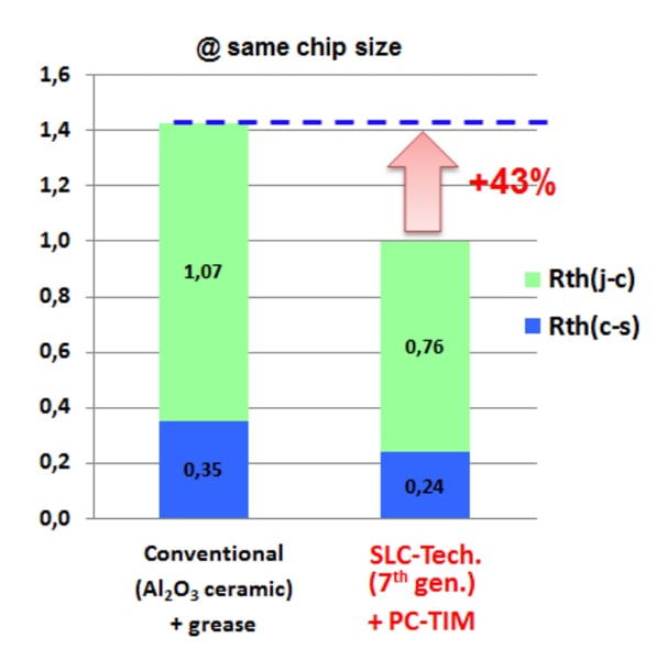
Figure 6: Comparison of thermal resistances at same chip size
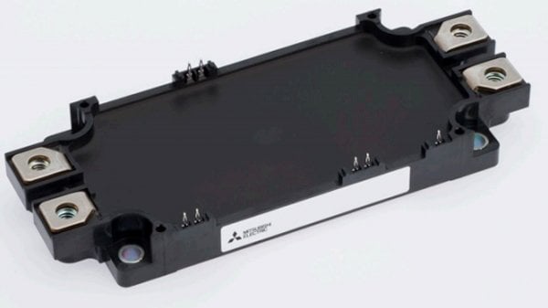
Figure 7: 7th gen NX-type 2in1 IGBT Module
7th Gen NX-type IGBT Modules
The new SLC-technology together with the 7th Gen IGBT chipset is introduced in the NX-type Modules Series of Mitsubishi Electric.
The 7th Gen IGBT chip has an improved trade-off of collector-emitter saturation voltage and turn-off switching losses. The cell design is optimized to have improved controllability of the dv/dt by the gate resistor. By using the RFC structure (Relaxed Field of Cathode) for the freewheeling diode it is possible to improve also the trade-off of recovery losses and forward voltage drop by keeping the soft recovery behavior [2].
The characteristics of the new chipset were evaluated and used for the simulation of losses with the Mitsubishi simulation software called MELCOSIM [1]. The result is that the 1200V class 7th Gen IGBT can save about 15% of total losses compared to the 6th Gen IGBT under typical motor control inverter application conditions.
To support the inverter assembly process on the customer side, all 7th Gen NX-type Modules will be available with the optimized PC-TIM and PressFit Pin terminals. Figure 8 shows that this NX-type 7th Gen IGBT Modules with SLC technology is under development with a comprehensive line-up to support a wide range of applications with these new technologies.

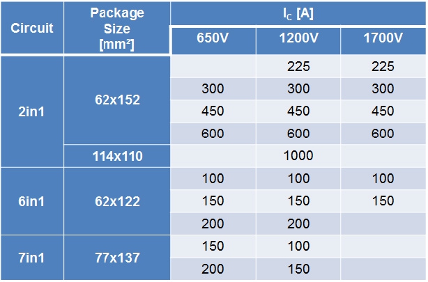 Figure 8: Line-up plan of 7th Gen NX-Type Modules with PC-TIM and PressFit options
System performance of 7th Gen Chipset and SLC-Technology
The features of 7th Gen Chipset from IGBT module point of view are explained above. But to understand the impact on the inverter system, these features have to be evaluated by a mission profile which is representative for typical inverter-mode operation. For many applications, load cycles have to be considered for the mission profile. By a loss simulation with the IGBT and diode chip characteristics, this load profile can be transferred into a loss profile. From this loss profile with the thermal impedance, the temperature profile can be calculated. Finally, the lifetime can be predicted with the temperature profile in combination with the cycling capability curves from the modules [4].
In Figure 9, an example of normalized values is shown. From loss simulation by MELCOSIM, it is noted that the total losses of 7th Gen Chipset can be reduced by 15% compared to the previous generation. It means that the loss profile is reduced to 85%. As considering this 15% loss reduction and the approximate 30% improvement of the thermal resistance, the junction Tj swings can be reduced to 60% compared to the conventional module with aluminum oxide ceramics substrate and copper baseplate.
In case of applying same loss that Tj swings of a conventional module is 50K, Tj swings of SLC-Technology with 7th Gen chipset would be 30K. So the result of target power cycling curves with the reduced Tj swings is that more than 10 times higher lifetime compared to a conventional module can be reached by using the SLC-Technology with a combination of 7th Gen IGBT. Or in case of the same lifetime, the Tj swings with SLC-technology can be increased to about 57K which is equivalent to increased output power by more than 50%.
IGBT Modules with SLC Technology
A new series of Mitsubishi IGBT modules for 600V and 1200V rated voltage has been developed covering a wide current range based on the well-established NX-package style. The new IGBT module series combines the latest 7th generation IGBT and FWDI chips with an innovative packaging technology called SLC technology.
The new IGBT module series is enabling inverter designs with higher output currents, higher power density and improved reliability (increased power cycling life and increased temperature cycling life). It’s an excellent answer to the complex needs of state of the art inverter designs.
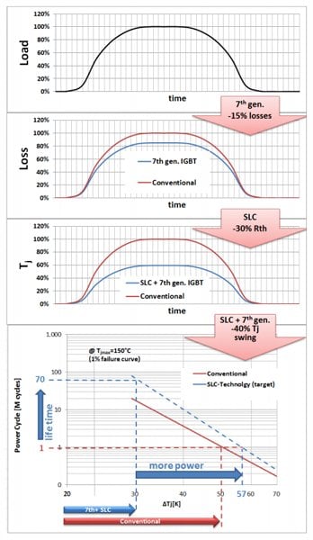
Figure 9: Normalized load cycle example with a comparison of SLC technology with 7th Generation IGBT and Conventional Module
About the Authors
Thomas Radke worked as an Assistant Manager Business Development Power Semiconductor at Mitsubishi Electric Europe - German. Mitsubishi Electric operates on the corporate principle of contributing to creating a vibrant and affluent society by enhancing its technologies, services, and creative powers, as a leader in the manufacture and sales of electric and electronic equipment used in Energy and Electric Systems, Industrial Automation, Information and Communication Systems, Electronic Devices, and Home Appliances.
Koichi Masuda worked at Mitsubishi Electric that operates on the corporate principle of contributing to creating a vibrant and affluent society by enhancing its technologies, services, and creative powers, as a leader in the manufacture and sales of electric and electronic equipment used in Energy and Electric Systems, Industrial Automation, Information and Communication Systems, Electronic Devices, and Home Appliances.
Reference
- MELCOSIM: IGBT thermal and loss simulation software, available at Mitsubishi Electric Power Module Loss Simulator.
- T. Radke; K. Masuda: “7th Gen. IGBT and Diode Chip-set Enabling Highest Performance Power Modules”, Bodo’s Power Systems June 2015, page 42-35
- Kota Ohara, et al: “A New IGBT Module with Insulated Metal baseplate (IMB) and 7th Generation Chips” , PCIM Europe 2015, page 1145-1148, ISBN 978-3-8007-3924-0
- 6.1th Gen S1 Series NX-Type Application Note, available at IGBT NX Note