Facebook
 Google
 GitHub
 Linkedin
Enhanced IGBT Module Power Density Utilizing the Improved Thermal Conductivity of SLC-Technology
This article introduces the new IGBT module generation of Mitsubishi Electric with improved Insulated Metal Baseplate as a key element of the SLC-Technology.
The 7th gen. Industrial IGBT modules have been successfully developed for the 650V and the 1200V classes to cover important power electronics system requirements such as high efficiency, high power density, and high reliability. The outstanding results pertaining to the thermal cycling capability, the “pumping out failure” free package, and the low thermal resistance of the SLC-Technology, combined with the low-loss 7th generation chipsets, are the key reasons for the success of the 7th gen NX-type IGBT modules. To expand this technology to 1700V class IGBT modules, the insulation capability and the thermal conductivity of the SLC-Technology’s IMB has been improved.
The 7th gen. 650V and 1200V class Industrial IGBT modules have been introduced recently to the market. In this new IGBT module generation, the latest chip technology has been employed to cover the requirements of industrial power electronics applications. All the applications utilize the superior characteristics of the 7th gen NX-Type IGBT modules which includes compactness, high power density, high reliability, high efficiency and reasonable cost. To expand the area of applicability to the 1700V class modules, the IMB (Insulated Metal Baseplate), which is a key element of the SLC-Technology, has been improved.
SLC-Technology with High Thermal Conductivity and Insulation Properties
The Al2O3 substrates are often used as the insulating layer in power modules. However, Mitsubishi Electric has employed the Aluminum Nitride (AlN) substrate in the previous generations, such as 5th and 6th gen. IGBT modules. Because of the superior thermal conductivity achieved by using AlN instead of Al2O3 the total thermal resistance Rth(j-c) between the chip and the baseplate was reduced by about 35% (see Figure 1).

Figure 1: Simulation result of thermal resistance Rth(j-c)
However, it is difficult to improve the thermal conductivity of ceramic any further. In addition, there is a stress experienced in the interconnection between the ceramic layer and the metal layer during thermal cycling due to the CTE (Coefficient of Thermal Expansion) mismatch of these materials (see Table. 1). However, using thinner ceramic substrates with the aim of improving the thermal resistance is not always the best approach. The thinner the substrate, the more sensitive it becomes against damages as a result of mechanical stresses. The SLC-Technology with the IMB structure has been developed to address this problem. A cross-section of this new structure is shown in Figure 2.

Table 1: Coefficients of Thermal Expansion CTE

Figure 2: Package structure of conventional and new 7th gen NX-type IGBT module with SLC-technology
By selecting the CTE value of the IMB’s insulating resin layer to be close to the CTE values of the top and bottom metal layers, the mechanical stress caused by the mismatch of the CTE values is reduced. Therefore, in comparison with the conventional structure using ceramic isolation substrates, the thickness of the insulating layer in the IMB can be reduced and the thickness of the metal layers can be increased respectively. With this approach, a thick metal layer can be chosen at the bottom side, substituting the metal baseplate and eliminating the large solder layer area between the baseplate and the ceramic substrate which is typical for conventional modules. As a result, the thermal resistance and the thermal cycling capability can be improved.
Compared to the surface area available for chip mounting at ceramic substrates, the surface area of the newly developed IMB can be enlarged because the size limitation known for ceramic substrates does not exist for IMB. In eliminating this size limitation, it provides flexibility in designing the size and the shape of the IMB. As a result, a higher chip mounting density in the module can be achieved by eliminating the interconnecting wires between the multiple isolation substrates. In addition, the thickness of the topside metal layer can be increased resulting in a reduction of the electrical lead resistance. This allows for designing the top side metallization pattern with narrower current traces, which helps in further increasing the area available for chip mounting and thereby increasing the power density of the module.
A second positive result obtained by employing an increased thickness of the topside metal layer is associated with the heat spreading effect which in-turn facilitates a further reduction in the thermal resistance “Rth(j-c)” and a reduction in the transient thermal impedance “Zth(j-c)” by virtue of the enhanced thermal capacity.
Optimization of IMB Properties for Higher Isolation Voltage
The complete line-up of 7th gen NX-type IGBT modules is shown in Table 2. The isolation voltage of 650V and 1200V class modules is specified as Viso=2,5kV AC 1min, while the isolation voltage of 1700V class module is at Viso=4kV AC 1min.
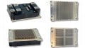
An example of the module package is shown in Figure 3. The same package size (62mmx152mm footprint) is used for the 600A 2in1 modules for the 650V, 1200V and 1700V voltage classes.

Table 2: Line-up of 7th gen NX-type IGBT modules

Figure 3: Package outline of 600A 2in1 NX-type IGBT module for 650V, 1200V and 1700V
The IMB had to be improved after reaching the same 600A rated module current at Vces=1700V and Viso=4kV in the same package size (62mmx152mm footprint). It was necessary to increase the specific thermal conductivity of the insulating resin layer so that it can compensate for the additional thickness of the insulating layer needed for Viso=4kV.
The insulation layer of the IMB consists of resin and ceramic particles. In order to achieve an improvement in thermal conductivity, it is necessary to increase the area of the heat-conducting path within the isolation layer, which is represented by the ratio of the ceramic particles to the resin quantity. If the ratio of the ceramic particles to the resin quantity is increased, the quantity of resin shrinks. The reduced resin quantity results in lower viscosity and consequently increases the requirement for employing a higher pressure during the IMB manufacturing process (required to remove voids). If the particle volume concentration exceeds a critical value, the dielectric breakdown voltage capability and thermal conductivity decrease as a result of voids in between the ceramic particles. The number of ceramic particles, resin quantity and the distribution of the ceramic particle size needs to be optimized to reduce voids, maintain high fluidity and the requisite press force at the sheet molding. As a result, the voids are eliminated and the quantity of ceramic particles in the insulating resin layer is increased. With this optimization, it becomes possible to enhance both the thermal conductivity and the withstand voltage characteristics.

Figure 4: Measurements result of IMB thermal resistance with different thickness
Figure 4 shows the measurement result of the thermal resistance of the IMB versus the resin insulating layer thickness. The total thermal resistance of the IMB is approximately 35% better compared to the conventional IMB because the thermal conductivity of the resin insulation layer is enhanced by 50%. The new IMB’s partial discharge inception voltage (PDIV) shows almost the same dependency on layer thickness as the conventional IMB. Thus, the proposed IMB has been confirmed to have equivalent PDIV and insulation characteristics while possessing an improved thermal conductivity.

Figure 5: Example of the improved 1700V IGBT module by the new IMB
An example of the achievable package size reduction by improved IMB is shown in Figure 5. For the previous 6th and 7th generation 600A/1700V 2in1 modules, the package footprint was 114mmx114mm and 62mmx152mm, which corresponds to a 49% reduction.
Figure 6 shows a summary of the new and the conventional IMB characteristics. It was validated that the thermal resistance of the new IMB for the 1700V module is approximately 5% better than the conventional IMB for the 1200V module.

Figure 6: Comparison of thermal resistance Rth(j-c) ratio
On the other hand, the new IMB could also potentially reduce the thermal resistance for the 650V and 1200V class IGBT modules. A combination of low loss 7th generation chips and the proposed improved SLC-Technology would enable us to further increase the current density of the modules. This option is currently under investigation.
The High Thermal Cycling Capability
The SLC-Technology utilizes layers with matched CTE-values as described previously. Additionally, the epoxy resin encapsulation can reduce the strain on the solder layer under the chip. This ensures higher reliability during heat cycling and thermal cycling. Figure 7 shows the Scanning Acoustic Tomography (SAT) images by heat cycling test (-40~+125 deg.C) at initial with 300 cycles and 600 cycles. The conventional structure had a degradation of the solder layer under the ceramic substrate after 300 cycles. On the other hand, the new structure with the DP encapsulation has the solder layer only under the chip and has no degradation after 600 cycles were observed. The result is the effects of the elimination of the substrate solder layer and the utilization of the epoxy resin layer.

Figure 7: SAT images at the different number of cycles
Figure 8 shows the result of the thermal cycling test (ΔTc=80K (+45~+125°C)). The newly developed structure was tested up through 40k cycles and has not failed yet. On the other hand, the conventional structure had degradation of the solder layer under the substrate (similar to the result of heat cycling). From this result, the new package with DP resin and IMB increases the thermal life cycling dramatically compared with the conventional structure. This aspect is contributed by eliminating a solder layer under the insulator, thereby reducing the strain of solder layer under the chips.

Figure 8: Thermal cycle test result of the SLC-Technology
SLC-Technology Offers a ‘Pumping-Out-Failure’ Free Package
The thermal resistance between the junction and the case has been successfully reduced by the improvement of the IMB. To achieve a higher power density and a high reliability, the thermal resistance Rth(c-s) between the base plate and the heatsink must be optimized.
In general, thermal interface materials are applied between the base plate of the module and the cooling fin to get an enhanced thermal contact. It must be noted that its parameters (such as thickness, performance, material property) have an impact on the heat dissipation capability and reliability. On the other hand, it is well known that the shape of the base plate of the power module is deformed by temperature changes generated by power losses in the IGBT- and Diodes-chips. This small but repetitive deformation of the base plate pushes out the thermal interface material, and is referred to as the “pumping out phenomenon”. For assuring a long-term stability in the thermal interface material, it is required to develop an advanced package structure which is capable of preventing the warpage of the base plate under continuous temperature cycles.
The conventional structure of the power module is shown in Figure 2 and its components along with the coefficients of thermal expansion (CTE) are described in Table. 1. In this structure, ceramic, solder and copper base plate, which are the constituents of the module base, have different CTE-values. When the case temperature changes with the heat generated by the various IGBTs / FWDs operation, each component expands and contracts to different extents due to the different CTE-values. Finally, among the various layers, the differential strain results in the differential deformation, such as with typical bimetal structures. This phenomenon is the cause of the base plate warpage.
The repetitive temperature change in a power module creates a repetitive warpage of the base plate as shown in Figure 9 (a) and (b). This warpage pushes out the thermal interface material. This pumping out phenomenon results in an ineffective thermal contact between the base plate and heatsink. This causes the degradation of Rth(c-s) and the heat dissipation capability of the power module. The consequence will be an accelerated aging of the power module, which, in the worst case, results in the thermal destruction of the module when the junction temperature exceeds the absolute maximum rating.

Figure 9: Phenomenon of baseplate warpage
The new package structure can dramatically reduce the differential strain between the component materials of the module by matching their CTE-values. The internal structure of the package and their CTE-values are described in Table 1 and Figure 2 respectively. This well-balanced (with respect to the CTE-values) structure results in much less deformation of the base plate caused by temperature change in comparison with a conventional structure. Figure 10 shows the result of the stress analysis (finite element method) for the base plate components (conventional and new structure respectively). The magnitude of the displacements shown in Figure 10 has been enlarged by the same factor in order to make the differences more visible.

Figure 10: Finite element simulation results of baseplate warpage
The simulation results depict that the new structure with the resin material has an improved response with respect to the base plate deformation during temperature changes.
For experimental verification, the vertical displacement of the baseplate center point was measured at three different ambient temperatures controlled by an environmental chamber also called a climatic chamber. The reference length was 91mm in the longitudinal direction. The displacement measured during the temperature change from 25°C to 125°C resulted in the only 13.4μm, which means that there was no significant warpage of the base plate. In the actual evaluation with a typical thermal interface material, no pumping out was found after 300 heat cycles (-40°C ~ +125 °C).
It is confirmed that the new power module structure, which has a matched coefficient of thermal expansion between adjacent layers, is able to minimize the warpage of base plate during temperature cycling and thereby provide a substantial reduction of the possibility of a pumping out failure event.
Summary
The improved SLC-technology enables an expansion in the line-up of the 7th gen. NX-series IGBT modules to the 1700V class by utilizing the higher insulation voltage and the superior thermal conductivity of the improved IMB. This technology enables the development of a 600A/1700V module with a 122x62mm² footprint.
The SLC-Technology also offers a drastically improved thermal cycling capability in combination with the elimination of the pumping-out failures. The 7th gen chips provide excellent efficiency by the reduction of power losses. By combining this chipset with the SLC-technology, the newly developed 7th gen NX-series IGBT provides an excellent answer to the requirements of power electronics systems such as high efficiency, high power density, and high reliability.
About the Authors
Thomas Radke is a Senior Application Engineer at Mitsubishi Electric Europe B.V, a company branch of Mitsubishi Corporation that focuses on electronics and electrical equipment manufacturing located in Ratingen, Germany. He earned his Bachelor's degree in Electrical Engineering and Electronics at Fachhochschule Düsseldorf (University of Applied Sciences - Dusseldorf). He also acquired his diploma in Associate Engineer in Automation Technology at Siemens Technology Academy - Düsseldorf.
Narender Lakshmanan works as an Application Engineer at Mitsubishi Electric Europe B.V, Ratingen, Germany. He is responsible for power semiconductor-based power converter solutions and has past roles which include project management of EPC projects. He earned his Bachelor's Degree in Electrical Engineer at Anna University, Chennai, Tamil Nadu, India. He then acquired his Master's degree in Electrical Power Engineering at RWTH Aachen University, Aachen, Germany.
Takuya Takashi and Shinsuke Asada both works at Mitsubishi Electric Corporation, a Japanese multinational electronics and electrical equipment manufacturing company headquartered in Tokyo, Japan. It is one of the core companies of Mitsubishi. Power device works are specialized and concentrated at the Fukuoka Branch of the Corporation.
References
- T. Radke et.al. “7th gen. IGBT and Diode chipset enabling highest performance power modules”, Bodo’s Power Systems, June 2015, p.30-32
- T. Radke et al., “More Power and Higher Reliability by 7th Gen. IGBT Module with New SLC-Technology”, Bodo’s Power Systems, August 2015, p.30-32
- T. Takahashi, et al: “A 1700V-IGBT module and IPM with new insulated metal baseplate (IMB) featuring enhanced isolation properties and thermal conductivity”, PCIM Europe 2016
- S. Asada, et al: “Resin Encapsulation Combined with Insulated Metal Baseplate for Improving Power Module Reliability”, PCIM Europe 2016,
- J. Yamada, et al:”Pumping out failure free package structure”, PCIM Europe 2016,
This article originally appeared in the Bodo’s Power Systems magazine.