Facebook
 Google
 GitHub
 Linkedin
Current Progress at Si IGBTs in the Voltage Range up to 1200V
In recent years the basic features introduced at the turn of the millennium for IGBTs such as trench gate cell and field stop layers could be enhanced.
In recent years the basic features introduced at the turn of the millennium for IGBTs such as trench gate cell and field stop layers could be enhanced. Progress in the manufacturing processes enabled reduced cell pitch for trench IGBTs leading to significantly lower on-state losses and improved switching behaviour. At the same time boundary conditions from the applications became clearly visible as hurdles for the further improvement even of silicon-based power switches and for reducing losses.
Preface
For the user, the question for the best-suited power switch for an application always stays important. This question will be considered here from a technical perspective in the light of new levels of development of Si IGBTs. In the focus are rated blocking voltages from 600V to 750V. The properties of these components may be extrapolated at least partly to higher voltage classes depending on the target application.
The “Ideal“ Power Switch
The losses occurring in the operation are an essential aspect for power switches. Therefore, the losses in conduction and blocking mode should be minimized. The switching losses, however, are determined by the overlap in time of voltage and current at the switch and therefore by the allowed switching transients in the application [1]. The losses for driving high voltage devices are much smaller than the switching losses on the power side and will be neglected here.
Figure 1 illustrates the idealized hard turn-off and turn-on of a power switch, where parasitic elements were not taken into account. If boundary conditions of the application limit the switching transients for voltage and current (dv/dt, di/dt) the ideal switch for an application thus possesses minimum achievable switching losses. The minimum switching losses may be easily estimated from the integral of the product of voltage and current at the switch.
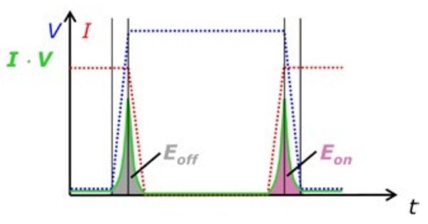
Figure 1: Schematic, idealized turn-off and turn-on neglecting parasitic elements.
The ideal switch for an application, therefore, has only these losses in operation which are determined by the allowed switching transients. So, a further reduction of switching losses is only possible to that extent the application may accept steeper switching transients. These limitations apply independently from the type of the power semiconductor switch and are valid for all base materials as silicon or wide bandgap materials.
Real IGBTs
In the blocking voltage range above 600V IGBTs are used as power switches for decades. Significant innovations have been introduced shortly before the turn of the Millennium which influenced the development of IGBTs – the combination of trench gate cells and vertical optimization using field stop layers at IGBTs. These innovations enabled to considerably reduce switching and conduction losses.
In power semiconductors, the chip area required in an application and thus the cost of the semiconductor devices are predefined by the power dissipation in operation. A larger chip area improves the heat flow from chip to ambient assuming otherwise same thermal boundary conditions in the setup.
Cost reduction for the semiconductor switch through a smaller chip area is possible only via reducing the losses in the switch.
The development of current power semiconductors has progressed so far that often no longer the semiconductors but the application limits the switching transients and thus dominates the switching losses. The development, therefore, has one focus on the reduction of on-state losses.
Reducing Losses of IGBTs
At IGBTs the on-state properties are improved by flooding a low doped zone needed to support the blocking voltage with electrons and holes. At the transition from on-state to blocking operation removal of this excess charge causes switching losses. The conduction losses could be reduced by introducing cells with trench gates. Optimizing the vertical structure (mainly field stop layers in combination with weak emitters at the collector side) helped to reduce both conduction and switching losses. Trench field stop IGBTs are dominant in the power semiconductor market today and have replaced older generations (punch-through- or non-punch through IGBTs) in most applications.
Reducing on-state Losses
Enhancements in the manufacturing processes allowed fine structures also for power transistors and thus trench cells with smaller cell pitches and narrow mesas in between the gate areas. It is possible to further increase the carrier concentration below the emitter electrode compared to conventional trench cells (Figure 2) by constraining the flow of holes of the excess charge through the p-body to the emitter electrode. The strong carrier storage below the emitter electrode leads to a significant increase in the electrical conductivity in the drift zone and thus improves the forward voltage [2] when compared to a classical IGBT with trench cells (Figure 3). Particularly noteworthy is that the nominal voltage of the IGBTs with narrow mesas in Figure 3 with 750V is even 100V higher than that of the classic trench-field stop IGBT consulted for comparison.
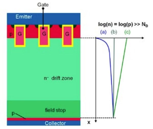
Figure 2: Vertical structure and carrier distribution at an IGBT with narrow mesas (c) compared to IGBTs with planar cells (a) and classical trench cells (b).
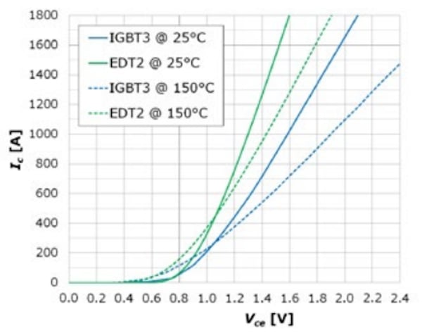
Figure 3: Comparison of the on-state voltage drop of an IGBT with narrow mesas (EDT2) and a conventional trench field stop IGBT (IGBT3).
The carrier gradient leads to an electron diffusion current through the drift zone which contributes to the total current. Thus the necessary portion of drift current and therefore the voltage drop in the drift zone are reduced [3]. The fine structures of the trench cells can be used, for example, to adjust the capacitances between collector and gate or the adjustment of the ratio of the collector-gate - and collector-emitter capacitances. Already [2] introduced a way of not connecting individual semiconductor regions between trench gates or to realize regions at the gates without source doping. In this way, the transconductance of the IGBT or its short circuit saturation current, for example, can be adjusted to the needs of the application [5].
Reducing turn-off Losses
At turning-off of an IGBT, the electrons and holes must be removed from the flooded drift zone in order to build up a space charge area (SCA) in the depleted, low doped drift region. The electric field in the space charge area enables blocking of the applied voltage.
In Figure 4 the conditions in an IGBT with narrow mesas are schematically shown at an arbitrary time during turn-off. The excess charge in the drift region is already partially removed, with the holes being removed through the space charge area to the p-body regions and finally to the emitter electrode. The positive charge of the holes travelling through the electric field in the space charge area causes switching losses.
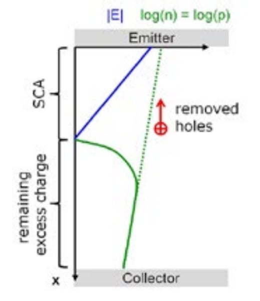
Figure 4: Schematic view during turn-off: removal of the remaining excess charge after on-state operation and building up the electric field/space charge area (SCA) to support the blocking voltage.
From Figure 4 it can be seen that IGBTs with narrow mesas remove the high hole concentration under the emitter electrode a blocking. The switching losses of IGBTs with narrow mesas in comparison to a conventional trench-field stop IGBT rise only slightly or not at all despite the significantly improved on-state properties. In any case, a more favorable operating point between conduction and switching losses will be found.
The electrons of the excess charge flow to the collector electrode at the rear side through the remaining, highly conductive remaining excess charge. Their charge is removed via an area that is practically free of electric field so that they contribute only indirectly to the turnoff losses because they cause additional injection of holes from the rear side emitter.
![Turn-off losses and on-state voltage at an IGBT with narrow mesas (EDT2) compared to a conventional IGBT (IGBT3) [2]](https://eepower.com/uploads/thumbnails/1981-4706-infineon-technologies-ag.jpg)
Figure 5: Turn-off losses and on-state voltage at an IGBT with narrow mesas (EDT2) compared to a conventional IGBT (IGBT3) [2]
The relationship between on-state and turn-off losses is exemplarily shown in Figure 5, in which of course also at the conventional IGBT the ratio between on-state and switching losses can be varied, albeit at a less favorable area.
In [4] different paths of optimization for finely structured IGBT cells are shown in combination with variations in the vertical concept and especially with a targeted, well-adjusted p-emitter on the rear side of the IGBT.
From Figure 4 it appears that weaker p-emitters result in a lower attachment point for the excess charge density on the collector side end of the drift zone and thus lower turn-off losses, because when switching off, fewer holes need to take the lossy way through the SCA.
In this way, the concept allows to adjust IGBTs with narrow mesas for a wide variety of target applications, ranging from the classical drive applications, resonant topologies up to fast switching applications, which are today mainly addressed by MOSFETs.
For chip versions with low density of the excess charge in front of the collector electrode, switching losses can be achieved that can compete even with older generations of superjunction MOSFET under comparable operating conditions.
During the turn-off of an IGBT, the slope of the current must be limited because in combination with stray inductances in the setup a peak overvoltage is generated. This voltage peak must not exceed the allowed blocking voltage limit of the IGBT in use. The current slope during turn-off is related to the excess charge density in front of the collector, and thus with the p-emitter. As shown in Figure 5 with the two more extreme designs, the turn-off loss between the weak and the strong p-emitter configuration is increased by approximately 1/3 while the forward voltage drops at the same current only by approximately 0.1V. Therefore, it is particularly advantageous for IGBTs with narrow mesas when their circuit surrounding, mainly the DC link, the IGBT package and the wiring, has particularly low stray inductances. During turn-off, steeper current transients may be acceptable allowing the choice of an IGBT with narrow mesas having lower p-emitter efficiency and thus lower overall losses.
All IGBTs which exhibit a maximum of excess charge density below the emitter electrode on the front side of the chip have a slightly increased turn-off delay time while the high carrier density below the emitter electrode is reduced. During this turn-off delay time, no significant losses occur because the voltage at the terminals of the IGBT is still near its saturation voltage. Future components which are closer to the limits for IGBTs described in [3] for physical reasons will have further increased turn-off delay times due to the distribution of the excess charge carrier density.
Turn-on Behavior
During hard turn-on in many cases, other requirements of the circuit and application define the maximum slope in the change of load current at the IGBT (diC/dt). Among these are in particular the fulfillment of electromagnetic compatibility (EMC) regulations and avoiding excessive voltage peaks due to the current slope in combination with parasitic inductances elsewhere. Using the IGBT, for example, in a bridge circuit, too high diC/dt may also lead to a snap-off of the corresponding free-wheeling diode. Also, the voltage drop during turn-on (dvCE/dt) must not exceed limits defined by the application. The turn-on behavior of IGBTs therefore in many cases is slowed down using gate resistors. The slower transients in diC/dt and subsequent dvCE/dt according to the collector gate feedback capacitance results in increased turn-on losses.
Switched-mode power supplies, which allow for fast current and voltage transients and where low switching losses are important, current IGBTs are combined with SiC Schottky diodes. This avoids a part of the switching losses caused by the stored charge of bipolar diodes.
Summary and Outlook
In recent years, the on-state characteristic of IGBTs could be improved by the use of modern semiconductor processing technology. In any case, the on-state performance of modern silicon devices is still far from the physical limits or dimensioning rules for the application as published previously [3]. Several generations of IGBT devices will follow with further optimized on-state and switching properties.
For many hard switching applications, limits are given for the permissible current and voltage rise and fall rates during switching. As a consequence, minimum possible switching losses are defined.
Already state-of-the-art silicon devices in many cases show faster switching than present applications allow – or could be designed for applications allowing significantly faster switching.
The switching properties of current IGBTs with narrow mesas can be adjusted specifically on a wide variety of applications. In variants for low switching losses, they can replace conventional or even slower switching superjunction MOSFETs in some applications. Even in design variants adjusted on prescribed current rise/fall rates, they provide a significant reduction in the conduction and switching losses compared to classic trench-field stop IGBTs.
About the Author
Anton Mauder received the Dipl.-Ing. degree in electrical engineering and the Dr.-Ing. degree from the Technical University Munich, Munich, Germany, in 1992 and 1996.,In 1996, he joined Infineon Technologies AG, Munich, Germany, as an R&D Engineer for IGBT modules. In 1998, he switched to the technology development group for power semiconductors.
References
- Wolter, F., Rupp, R., Häberlen, O.: Next level Silicon, SiC and GaN – a balanced view on future power semiconductor switches. Proceedings of APE – Congress on Automotive Power Electronics, Paris, 2015.
- Wolter, F., Rösner, W., Cotorogea, M., Geinzer, T., Seider-Schmitt, M., Wang, K.-H.: Multi-dimensional trade-off considerations of the 750V Micro Pattern Trench IGBT for Electric Drive Train Applications. Proceedings of the 27th ISPSD, Hongkong, 2015, p. 105- 108.
- Nakagawa, A.: Theoretical Investigation of Silicon Limit Characteristics of IGBT. Proceedings of the 18th ISPSD, Naples, 2006, p. 5-8.
- Kimmer, T., Griebl, E.: Trenchstop 5: A new application specific IGBT series. Proceedings PCIM Europe 2012, Nürnberg, 2012, p. 120-127.
- Jäger, C., Philippou, A., Vellei, A., Laven, J. G., Härtl, A.: A new sub-micron trench cell concept in ultrathin wafer technology for next Generation 1200 V IGBTs. Proceedings of the 29th ISPSD, Sapporo, 2017, p. 69-72.
This article originally appeared in the Bodo’s Power Systems magazine.