Facebook
 Google
 GitHub
 Linkedin
CoolSiC MOSFETs A Revolution to Rely On
This article highlights Infineon Technologies AG SiC MOSFETs standard IGBT driver voltages and switching behavior that enables a very low design effort.
The Silicon Carbide (SiC) switches are increasingly popular for power converters and other power-related applications. This latest technology delivers higher efficiency, faster-switching frequencies, reduced heat dissipation and space savings which sums up to lower overall costs.
The Infineon’s latest CoolSIC™ MOSFETs was launched at PCIM on May 2016 under the banner of ‘A revolution to rely on’. The device offers designers unsurpassed power density and performance. Here we look at this technology and introduce an integrated CoolSIC-based reference design.
CoolSiC Applications Now and in the Future
Certain application segments will always be early adopters of any new technology. There are several factors that trigger designers to migrate to a new technology some of this including the system value, the cost, and the performance ratio. The SiC Schottky diodes are already used extensively in high-end power supplies. Looking forward, Infineon believes solar inverters and boost circuits will gain the most from MOSFET technology, quickly followed by uninterruptible power supplies (UPS) and chargers. Traditional segments such as motor drives, traction and, on a longer time scale, automotive applications are expected to embrace a large-scale migration to the new semiconductor technology in the future.
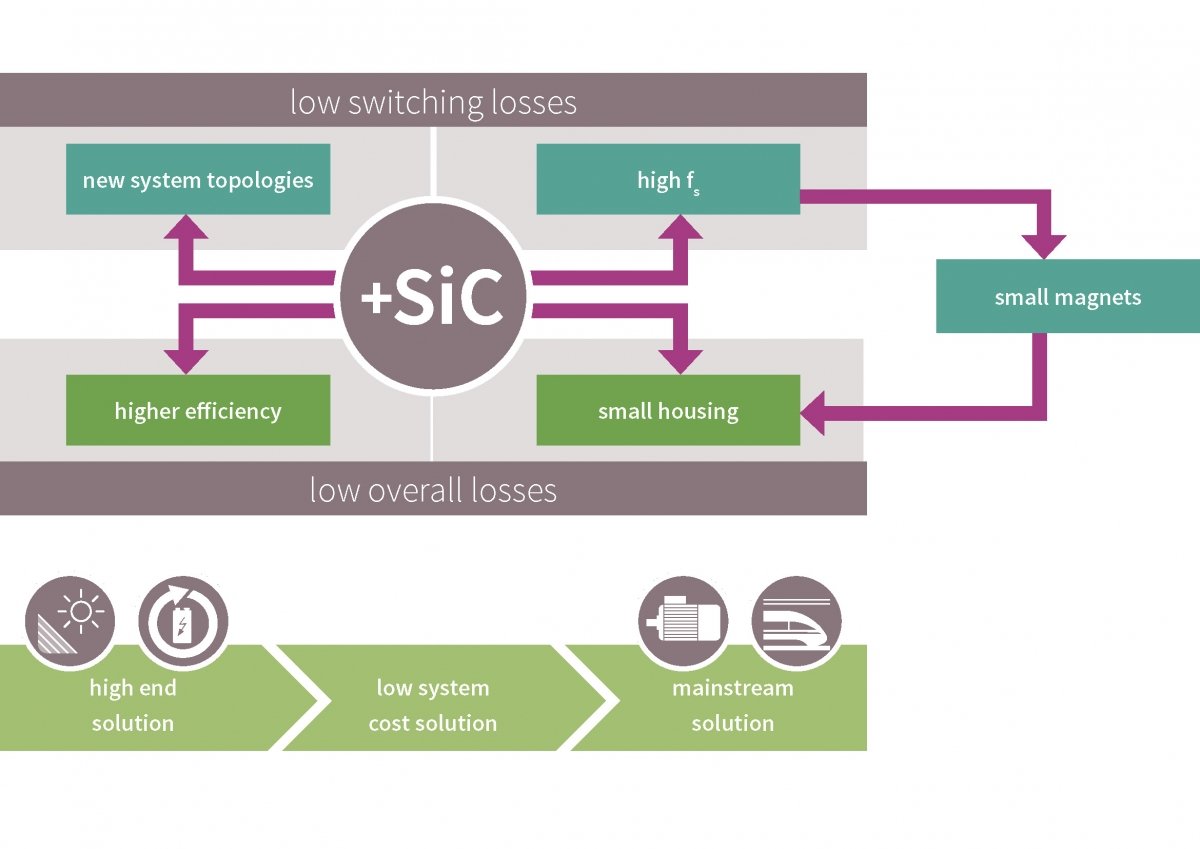
Figure 1: SiC benefits and target applications
The most significant trend in solar inverter designs is the increasing power density based on the reduction of switching losses, thereby enabling smaller heatsinks. Associated with this are the higher operating frequencies that enable smaller magnetic components.
CoolSiC MOSFET Solutions
CoolSiC MOSFET devices with an ON-resistance (RDS(ON)) of 45 mΩ are an important step for SiC in power semiconductors. However, the IGBTs and SiC transistors must consider the equal importance of both performance and package design. That’s why Infineon has developed a broad portfolio of packages.
By using the 4-Pin TO-247 (IMZ120R045M1) instead of the standard 3-pin TO-247 device (IMW120R045M1) it is possible to have a dedicated Kelvin source pin. As a result, the gate control voltage is not impeded by the load current flowing in the power source pin and improves turn-ON losses by up to 40%.
These discrete leaded products are ideal for fast switching applications and the earliest applications adapter includes photovoltaic (PV) string inverters, chargers, and UPS equipment.
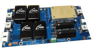
Alongside discrete packages, the popular and flexible Easy1B power module is used to implement a half bridge configuration and booster solutions optimized for PV. These modules include 1200 V CoolSiC Schottky diodes and low VF silicon diodes for bypass and inverse-polarity protection. Besides the <10 nH stray inductance, the flexible pin grid of Easy modules makes PCB layout easier. This is a factor-of-five improvement over previous solutions and represents a valuable step in power module design. The booster module is the size of a matchbox and is designed to be used in MPP tracker systems up to 20 kW.
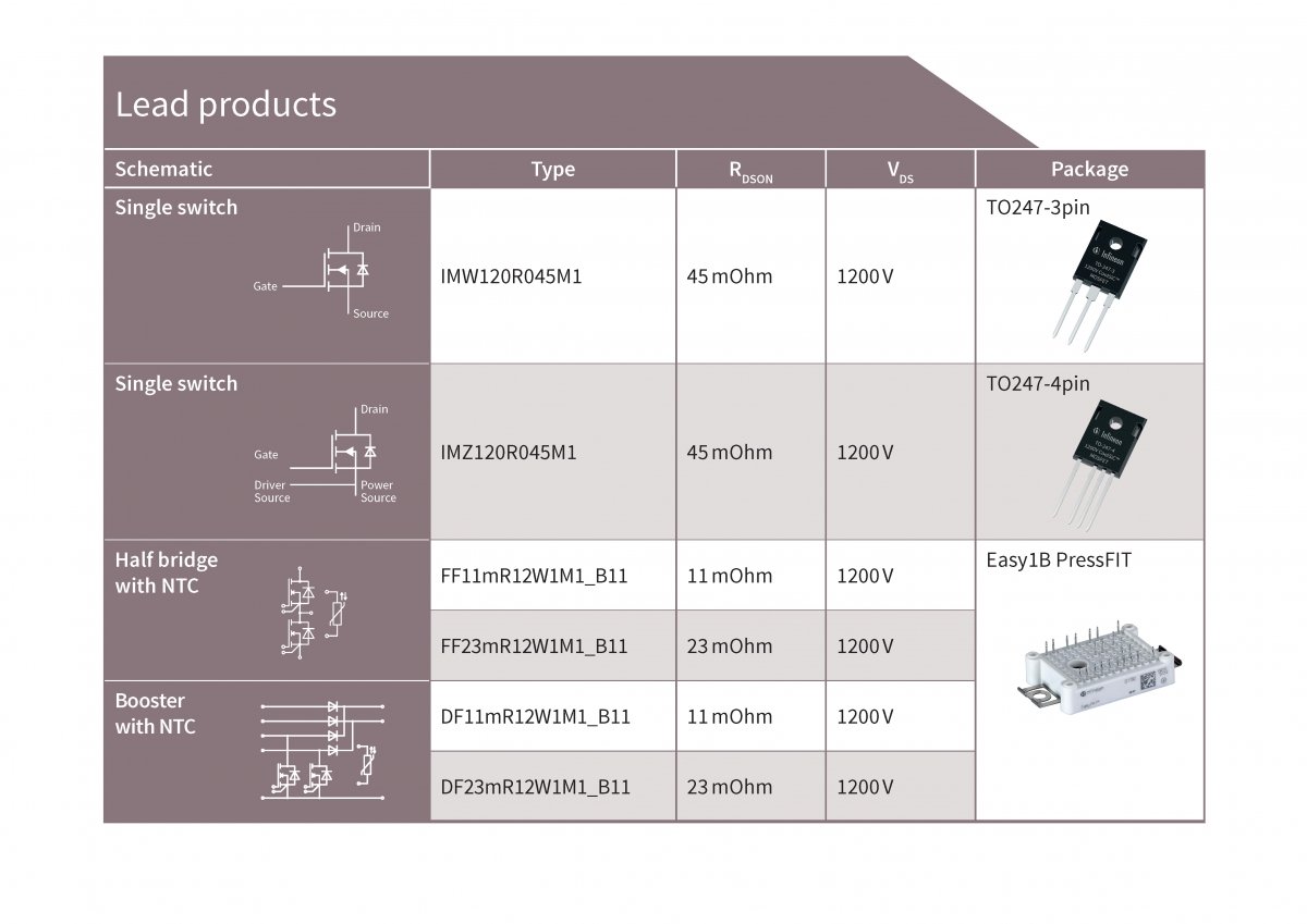
Figure 2: CoolSiC MOSFET lead product overview
The key drivers behind the use of alternative semiconductor materials for power diodes and transistors are efficiency, power density, and cost. Hybrid power modules using silicon IGBTs and SiC Schottky diodes have become mainstream in power converters with high switching frequencies (>10 kHz) such as solar string inverters and UPS systems. Using EasyPACK™ and EconoPACK™ hybrid power modules and discrete packages, Infineon was able to address broad portfolio of CoolSiC Schottky Diodes by using SiC solutions that combine SiC diodes with transistors, achieving higher switching frequencies and conversion efficiencies.
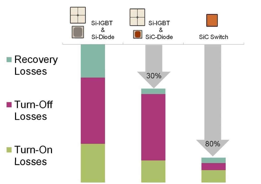
Figure 3: Evolution of loss reduction by the use of SiC power devices
The additional loss reduction of about 50 % resulting from the transition to full SiC is the result of a lower turn-OFF and ON-state losses.
On the one hand, current SiC MOSFETs do require special drivers in combination with non-standard driving voltages, leading to low market adoption. On the other hand, the new Infineon CoolSiC MOSFET uses standard IGBT driving voltages (e.g. -5 V/15 V or -0 V/15 V) which allows the use of standard gate driver IC’s such as the EiceDRIVER™ Compact and enables widespread adoption of SiC MOSFETs into power electronic systems.
Switching Behavior
Testing a 45 mΩ CoolSiC MOSFET in a TO-247 4-pin package driven with -5 V/15 V for its switching behavior results in very clean switching with almost no oscillations during switch ON. The benign behavior makes an easy and fast implementation of the CoolSiC into existing systems using standard EiceDRIVER IGBT drivers.
A DC/DC converter using a CoolSiC half-bridge module and an EiceDRIVER Compact with 6A output (1EDI60H12AH) was built for the evaluation of the switching behavior at the system level. It was configured in a bidirectional buck-boost converter topology and has an ohmic resistance (RDS(ON)) of 23 mΩ at room temperature (FF23MR12W1M1_B11).
To measure the dv/dt at a gate resistance of 1 Ohm and different drain currents a double pulse measurement was performed. Only a slight oscillation was observed during the switching at 5 A where the turn ON and turn OFF behavior was seen. This is shown in the upper chart of Figure 4. The dv/dt at turn-OFF has a relatively low value of 5 kV/µs. Meanwhile, the switching of CoolSiC MOSFET module at 600 V and 30 A is shown in the lower chart of Figure 4.
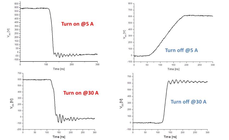
Figure 4: Turn ON and turn OFF of the CoolSiC module within a DC/DC converter at 5 A and 30 A
The dv/dt at turn-OFF is 34 kV/µs, which is much higher than for 5 A. The large output capacitance of the SiC MOSFET is the result of the strong dependence of the switching behavior on the drain current. The large displacement currents in the output capacitance of the device accelerate the turn-OFF by a dynamic increase of the turn-OFF voltage.
Further measurements of dv/dt and the peak voltage are shown in Table 1.
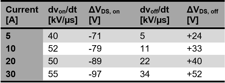
Table 1: dv/dt and Vpeak of VDS at different currents
Controllability
A further advantage of the CoolSiC MOSFET is the controllability of dv/dt and di/dt by adjusting the external gate resistors. The test results of the FF45mR12W1M1_B11 CoolSiC Easy1B half-bridge module is shown below.
Increasing the value of the external gate resistors can reduce the dv/dt and di/dt of the MOSFET. This technique helps to reduce electromagnetic noise or to fulfill application-specific requirements.
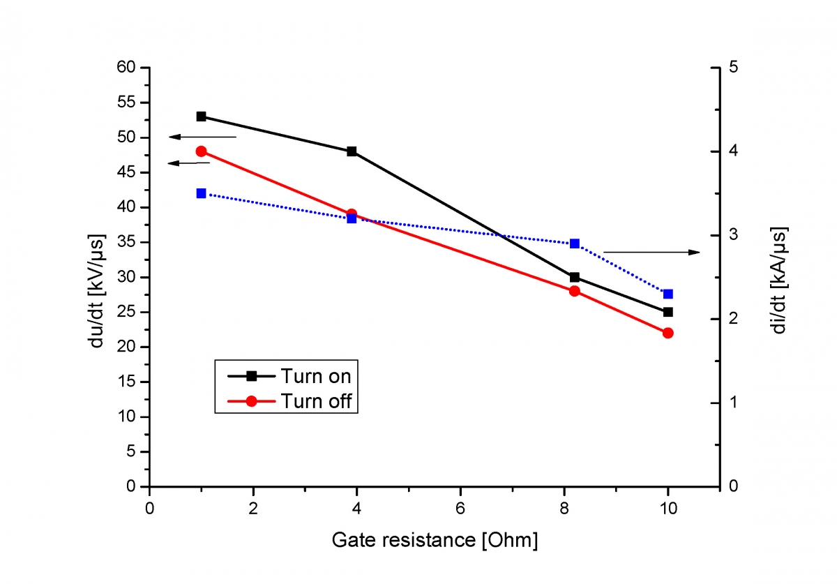
Figure 5: Controllability of the CoolSiC MOSFET via external gate resistors and the corresponding di/dt and du/dt levels
The dv/dt control allows the device switching performance to be tailored to match the requirements of a specific application. A common example relates to the restrictions regarding dv/dt limits for motor winding insulation (e.g. 5 kV/µs). By making the right choice for gate resistors the CoolSiC MOSFET restrictions are easily met and solved.
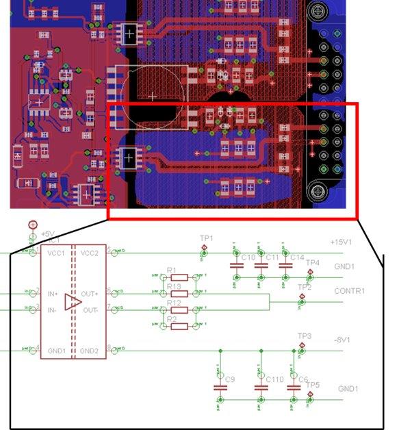
Figure 6: Example of a simple driver circuit for the CoolSiC MOSFET using Infineon’s new compact driver 1EDI60H12AH
Maintaining a very low inductance around the gate-source loop between the driver IC, the module gate and the auxiliary source pins is the primary challenge for the gate driver PCB layout. This can be achieved through the principle of a “stripline” design by using planes, and wide traces arranged in parallel paths. This enables a significant electromagnetic noise reduction especially in the context of hard switching with Rg=1 Ω.
It is very important to pay special attention to the PCB layout when obtaining maximum performance from CoolSiC MOSFETs, especially when minimizing inductive loops. The demonstration driver circuit is part of an evaluation system, designed to measure the performance of the CoolSiC module. This system has been run at operating frequencies up to 500 kHz.
Summary and Conclusion
Full access to the additional switching performance available when using Infineon SiC MOSFETs can be obtained with standard components and topologies.
Infineon CoolSiC MOSFETs have standard IGBT driver voltages and benign switching behavior, which enables a very low design effort, especially with respect to driver development. In addition, the easy controllability of the dv/dt through the use of external gate resistors (simplifying EMI management and ensuring excellent switching performance) results in a lower cost of development for high-performance power converters based on CoolSiC devices.
With the introduction of the CoolSiC MOSFET technology, the beginning of a new era of power electronics in terms of power conversion efficiency and power density has begun. Compared to the silicon IGBT based solutions, the CoolSiC MOSFET has great features which enables engineers to develop smaller and more efficient PV inverters, UPS, and charger systems that use higher switching frequencies and smaller heatsinks resulting in up to 80 % lower switching losses compared to silicon-IGBT-based solutions.
This article originally appeared in the Bodo’s Power Systems magazine.
About the Authors
Dr. Maximilian Slawinski works as the Head of Product Marketing Product Line High Power Modules at Infineon Technologies, where he is responsible for the business and PM team for high power module products covering all high voltage and high power modules within Infineon. He has earned 4 honors and awards throughout his career and has accomplished 7 publications as well. He earned his Engineering Dipolma in Electrical and Electronic Engineering, Master's Degree in Business and Engineering, and his Doctor's Degree in Electrical Engineering all at RWTH Aachen University (Rheinisch-Westfälische Technische Hochschule Aachen) located in Germany.
Marc Buschkühle works as the Head of the Technical Marketing High Power Modules at Infineon Technologies AG, Warstein, where he is responsible for the Technical Marketing team and products for High Power Modules covering high voltage (Voltages greater than or equal to 1.2 kV) and high power (greater than 200 kW) application within Infineon.