Facebook
 Google
 GitHub
 Linkedin
Digital Power Supply Loop Design StepbyStep Part 2
This article highlights Biricha’s digital power supply loop with digital linear difference equations that emulate analog Type II and Type III compensators.
In the previous article, we showed that the output of almost any op-amp compensator can be emulated in the digital domain with a single linear difference equation. We then created a simple op-amp integrator/compensator, presented its linear difference equation (LDE) in the digital domain and then plotted the output of the op-amp commentator vs its digital equivalent LDE. We saw that the output of our mathematical equation in the digital domain was almost exactly the same as the op-amp circuit in the analog world.
The vast majority of analog power supplies are compensated using only 2 different types of op-amp circuits: Type II or Type III. The design of these compensators is covered in detail both in theory and with hands-on labs in Biricha’s Analog Power Supply Design Workshops [1]. We have also discussed these in previous articles [2] in Bodo Power. If the vast majority of analog, PSUs are stabilized with only two different types of op-amp compensators. It follows, therefore, that the vast majority of digital power supplies can be stabilized with just two simple linear difference equations.
The digital equivalent LDE for a Type III compensator is called a 3-Pole, 3 Zero Compensator (3p3z) and the digital equivalent LDE fora Type II is called a 2-Pole, 2-Zero compensator (2p2z).
Biricha’s “Digital Power Supply Design Workshops” covers how these are derived and how you can design your own digital compensators in detail [3]. For the purpose of this short article, all we require is the digital LDE’s for these two popular compensators.
The Digital Equivalent LDE for an Analog Type III Compensator
The circuit diagram of a standard Type III compensator is shown in Figure 1.
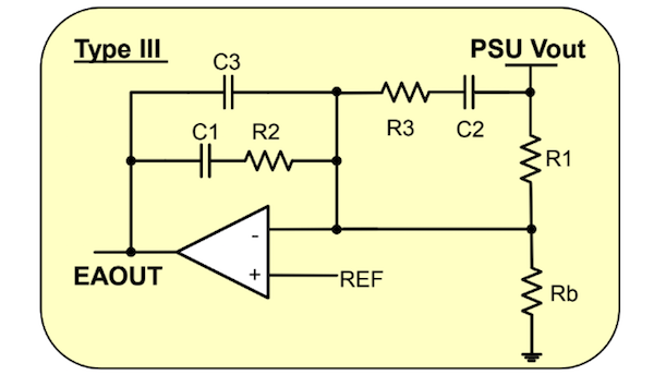
Figure 1: Analog Type III Compensator
From Biricha’s design workshops [1,3] and previous articles here [2], we know that this compensator has 3 poles and 2 zeros as shown in its transfer function Hc(s) below:
We can see that we have a pole at the origin, two more poles, and two zeros. Again from Biricha’s workshops and previous articles in Bodo, we know exactly how to place these poles and zeros in the analog world in order to get a stable loop with a desired cross-over frequency and phase margin. Please note all terms are in radians and all F terms are in Hz.
The digital equivalent LDE for this circuit is shown below:
Please don’t let the long equation put you off; we will explain everything shortly. This is called a 3-Pole 3-Zero digital compensator (3p3z) and every time in analog world we use a Type III in digital we must use a 3p3z to get a near exact performance. Please note that in digital we have an extra zero when compared to the analog.
Transformation from the Analog World to the Digital World
This is only an artifact of our transformation from the analog world to the digital world and therefore, the numerical output of this equation in the frequency domain is an almost exact replica of the analog op-amp in Figure 1. Just like the op-map integrator of the previous article, we are ignoring the impact of all scalings and time delays for now.
We know from our last article that y[n] in the equation above is our output from our digital compensator at this exact instance, i.e. the new value of demand PWM in this exact instant. We also know that x[n] is our input to the digital compensator at this exact instance, i.e. the error signal in this exact instant. In the case of a power supply, this is usually the difference between our real output voltage as sampled by the ADC and our demand/reference voltage.
We also know that y[n-1] means our previous output, i.e. from the last sampling interval. If we assume a switching/sampling frequency of 200kHz, then each sampling interval would be 5us. Therefore “previous output” would be the output of the compensator 5us ago.
Similarly, y[n-2] would be our “Previous Previous output” from 10us ago and x[n-3] for example, would be our “Previous Previous Previous input” from 15us ago and so on. Finally, you can see that the y terms are multiplied by a bunch of coefficients: A1, A2, A3, and the x terms are multiplied by another bunch of coefficients B0, B1, B2, B3.
These coefficients determine the locations of our poles and zeros. Ignoring all scalings and time delays for now, if we know the position of poles and zeros of our analog compensator (which we do), all we have to do to create an equivalent digital one is to calculate these 7 coefficients using the following equations:
I appreciate that at first glance these conversion equations may look big and intimidating, but the good news is that there is NOTHING within these equations that we do not know. We will now demonstrate this with a real-life numerical example.
Let us assume that we have designed an analog Type III compensator for a 200kHz Buck converter which has the following poles and zeros:
Fz1 = 1.21323 kHzFz2 = 1.61764 kHzFp2 = 6576.65 kHzFp3 = 100 kHzFp0 = 625 Hz
Where Fz1 and Fz2 are our zeros, Fp1 andFp2 are compensator pole and Fp0 is our pole at origin.
Coefficient (A1) Calculation
Let us now calculate our first coefficient (A1) from the equation above. Yes, I appreciate that this is a long equation but please have a look to see if there is anything in this equation that we do not know. We know everything!
Ts is our sampling interval and in our case is 5us for a 200kHz switching frequency and and are our compensator poles in analog world which we know to be Fp2 = 6576.65 kHz, Fp3 = 100 kHz (don’t forget to convert to radians).
Therefore, we can calculate A1 accurately to be 1.590703155656. Now please take a look at the other intimidating coefficient equations. As with the A1 equation, even though these are long equations there is nothing within them that we do not know and therefore we can easily calculate all of them. Substituting our analog poles and zeros into the above equation and setting Ts to 5us, we have:
B0 = (+1.212026610403)B1 = (-1.106625987416)B2 = (-1.209779932536)B3 = (+1.108872665284)A1 = (+1.590703155656)A2 = (-0.410251039699)A3 = (-0.180452115956)
New PWM duty
You can now see that we have a simple LDE, similar to the LDE of our previous simple op-amp compensator of the previous article and therefore we can easily get our MCU to calculate it. As a reminder our output y[n] is our new PWM duty and our input x[n] is the difference between the demand output voltage and the real measured output voltage from the ADC:
y[n] = A1 y[n-1] + A2 y[n-2] + A3 y[n-3] + B0 x[n] + B1 x[n-1] + B2 x[n-2] + B3 x[n-3]
Our design is complete and this equation should behave almost exactly the same as the analog Type III compensator with the aforemen-tioned poles and zeros.
The Digital Equivalent LDE for an Analog Type II
Compensator The circuit diagram of a standard Type II compensator is Figure 2.
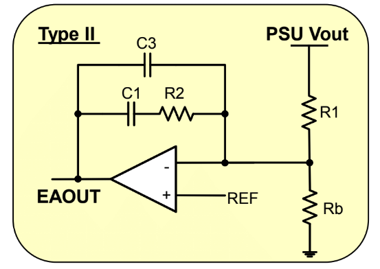
Figure 2: Analog Type II compensator
You can see that the only difference between a Type II and a Type III is the omission of R3 and C2 from the Type III circuit. All this means is that the transfer function of our Type II has one less pole and one less zero as shown:
The linear difference equation for the Type II in the digital world has 2 poles and 2 zeros and therefore it is called a 2-pole, 2-zero (2p2z) controller.
Any time in the analog world, we use a Type II in the digital world we can use a 2p2z
y[n] = A1 y[n-1] + A2 y[n-2] + B0 x[n] + B1 x[n-1] + B2 x[n-2]
Our 2p2z LDE only has 5 coefficients (instead of 7 for 3p3z). These are given below:
Again, even though the equations are long, you can see that provided that we have our poles and zeros in the analog world and our sampling interval Ts, there are no unknowns and we can calculate everything.
Impact of Scalings and Time Delays
The LDE that we derived is the digital equivalent of the op-amp transfer function, but there will be various elements within the digital power supply that add a constant scaling factor to the gain plot.
For example, if the maximum output of our power supplies is 6.6V and our ADC which samples it can only tolerate 3.3V then we have added a “divide by two” potential divider. This scaling factor of 0.5 needs to be taken into consideration or our gain bode plot and therefore our crossover frequency will be off by a factor of 0.5. Similarly all pure time delays, for example, the time taken from the time we sample our output voltage with the ADC to the time we update our PWM, add phase delays to our phase plot. Therefore, we will end up with less phase margin than we expected.
So far we have ignored the impact of various scalings and time delays. The good news is that all these are all easily calculated and we cover them all in the next article. We will also provide a step-by-step design and verify with complete experimental results.
Concluding Remarks
In this article, we introduced the digital linear difference equations that emulate analog Type II and Type III compensators. We provided all the equations necessary to calculate all the coefficients.
We proposed that although the coefficient equations can be big, provided that we know our analog poles and zeros and the switching/sampling frequency we can easily calculate them. To prove the concept, using a numerical example we showed exactly how all the coefficients can be calculated. Finally, we briefly discussed the impact of various scaling factors and time delays on our loop response in terms of gain and phase plots.
In the next article, we will detail exactly how to calculate and compensate for ALL scalings and phase losses to get a near-perfect match between analog and digital. We will then present a complete step-by-step numerical design example, implement this design in real life and provide experimental results to show that the theory matches with practice.
References
[1] Biricha Digital’s “Analog PSU Design Workshop” Handbook
[2] Previous Biricha Lecture Notes in Bodo Power Magazine
[3] Biricha Digital’s “Digital PSU Design Workshop” Handbook
About the Author
Ali Shirsavar is a Doctor of Philisophy (PhD), Power Electronics at the University of Reading, Berkshire, England. He is an Associate Professor at the University of Reading for more than 17 years, then become a Director in Biricha Digital Power.
Related Content