Facebook
 Google
 GitHub
 Linkedin
University of Arkansas Receives Grant for New SiC-Based Semiconductor Fabrication Facility
Researchers from the University of Arkansas receive a $17.87 million grant from the National Science Foundation to build and run a fabrication facility for silicon carbide-based semiconductor technology.
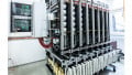
This month, Professor Alan Mantooth and his research team from the University of Arkansas received a grant of $17.87 million from the National Science Foundation (NSF) to build and operate a national silicon carbide (SiC) research and fabrication facility. The open-access facility will be an important base from which the U.S. can develop and produce integrated circuits made with SiC-based semiconductor technology.

SiC Technology
SiC is one of the most promising semiconductor materials. It has many advantages over silicon, which makes it a better option for semiconductor technology. SiC can be used in transistors, diodes, and capacitors to make circuits more powerful. The principal advantages of using SiC over other materials like Silicon are low leakage current, high speed, high power density, wide bandgap, radiation hardiness, and thermal stability.
Advantages of using SiC:
- SiC can be used in transistors, diodes, and capacitors to make circuits more powerful.
- The costs of manufacturing silicon carbide are lower than silicon.
- SiC is immune to thermal runaway because it has a negative temperature coefficient. This makes it a much safer material for use in semiconductors.
At present, fabrication facilities dedicated to SiC technology in the U.S. are for internal use only, and U.S. research and development (R&D) of SiC integrated circuits (ICs) relies on international fabrication. This is why a dedicated facility, such as the one intended to be built at the U of A is critical for the U.S. semiconductor industry and by extension the U.S. economy.
The New Facility
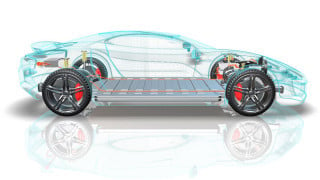
The new fabrication facility will be used to train and up-skill the next generation of semiconductor researchers and engineers, as well as enable the prototyping, proof-of-principle demonstration, and design of SiC-based semiconductors. The facility will focus on creating lighter, more energy-efficient ICs which can withstand high temperatures. In addition to ICs, the facility will be used to provide sensors and devices for military and industrial applications (such as solar inverters and electronics for cars). This will include those that are both electric and gas-powered. Components will also be provided for heavy transportation and construction equipment (such as bulldozers) and electronics developed for systems used in geothermal and space exploration.

Image used courtesy of U of A
In a recent news release, Mantooth commented, “The national impact of having a fabrication facility such as this is enormous.” Mantooth added, “The country that leads the world in advancing silicon carbide semiconductor design and fabrication will also lead the race to market nearly all-new game-changing technologies, including those used by the military, as well as general electronic devices that are essential to our economy.”
The development of the U of A facility will be an invaluable resource for research staff and students, as well as for the U.S semiconductor industry at large. Students at all degree levels and from underrepresented communities at the U of A will have the opportunity to engage in a highly desired area of science and technology.