Facebook
 Google
 GitHub
 Linkedin
ESiP Project Reaches Successful Completion under Infineon Leadership
The largest research project in Europe for researching and developing highly integrated system-in-package solutions has been successfully completed. The Efficient Silicon Multi-Chip System-in-Package Integration (ESiP) project partners have worked out future system-in-package solutions that are more compact and reliable. They have also developed methods for simplifying analyses and tests. Under management of Infineon Technologies AG, 40 research partners — microelectronics companies and research institutions — from a total of nine European countries worked together. ESiP was funded by public authorities of all nine countries and the ENIAC Joint Undertaking.
In order to strengthen Germany as a microelectronics location by promoting collaboration at European level, the German Ministry of Education and Research (BMBF), the largest contributor among the national ministries, supported the project as part of the German government's High-Tech Strategy. Among the German research partners, in addition to three institutes of the Fraunhofer-Gesellschaft, were the companies Cascade Microtech GmbH, Feinmetall GmbH, Infineon Technologies AG, InfraTec GmbH, PVA TePla Analytical Systems GmbH, Siemens AG and Team Nanotec GmbH.
“The successful ESiP research enhances Europe's position in the development and manufacture of miniaturized microelectronics systems,†says Dr. Klaus Pressel, ESiP project head and responsible for international cooperation on assembly and packaging solutions at Infineon Technologies AG. “With the ESiP findings we will be able to further miniaturize and improve microelectronic systems. We have developed new manufacturing processes and materials for SiP solutions along with methods for testing them, running a failure analysis on them and evaluating their reliability.â€
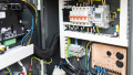
System-in-Package (SiP) means different types of chips made using different production techniques and structure widths are embedded side by side or stacked above one another in one chip package and work smoothly together. For one, technologies for combining chips in SiP packages and manufacturing them were developed and, for another, procedures for measuring reliability and methods as well as equipment for failure analysis and testing.
Basic technologies were developed that enable the integration of various types of chips in the smallest volume of an SiP package, for example, customer-specific processors with the latest CMOS technologies, light-emitting diodes and DC-DC converters, MEMS and sensor components and passive components such as miniaturized capacitors and inductors. The ESiP findings will enable future microelectronic systems to have more functionality while at the same time being considerably smaller and more reliable.
These compact SiP solutions will find application in e.g. electric vehicles, industrial applications, medical equipment and communications technology. With ESiP, not only were new production processes for SiP solutions developed with two or more very different chips in one package. New materials for building SiP solutions were also investigated. The research partners have proved the feasibility and reliability of the new production processes with more than 20 different test vehicles. Moreover, in the course of the research work it was confirmed that the test procedures commonly used today are no longer sufficient for future SiP solutions. That's why new test flows, probe stations and probe adapters were developed for 3D SiP.