Facebook
 Google
 GitHub
 Linkedin
Controlling the Crystal Structure of Gallium Oxide for Power Devices
Precise control of the atomic structure of gallium-oxide layers improves the development of high-power electronic devices. A simple method that uses hydrogen chloride can better control the crystal structure and shows promise for novel high-powered electronic applications.
The electronic components used in computers and mobile devices operate at relatively lower power. But high-power applications, such as controlling electrical power grids, require alternative materials that can cope with much higher voltages.
For example, an insulating material begins to conduct electricity when the field is high enough, an effect known as electrical breakdown. For this reason, power electronics often use nitride-based semiconductors, such as gallium nitride, which have a very high breakdown field and can be epitaxially grown to create multilayered semiconductors.
However, ever-increasing energy demands and the desire to make electricity distribution more efficient requires even more electrically robust materials. Gallium oxide (Ga2O3) has a theoretical breakdown field more than twice that of gallium-nitride alloys and so has emerged as an exciting candidate for this function. The latest challenge however is a simple way to deposit high-quality gallium oxide on the substrates commonly used for power electronics, such as sapphire.
Haiding Sun, Xiaohang Li, and co-workers from King Abdullah University of Science and Technology (KAUST) worked with industry partners Structured Materials Industries, Inc. in the U.S. to demonstrate a relatively simple method to control the crystal structure of gallium oxides on a sapphire substrate using a technology known as metalorganic chemical vapor deposition (MOCVD).
"We were able to control the growth by changing just one parameter: the flow rate of hydrogen chloride in the chamber," explains Sun. "This is the first time that hydrogen chloride has been used during oxide growth in an MOCVD reactor."
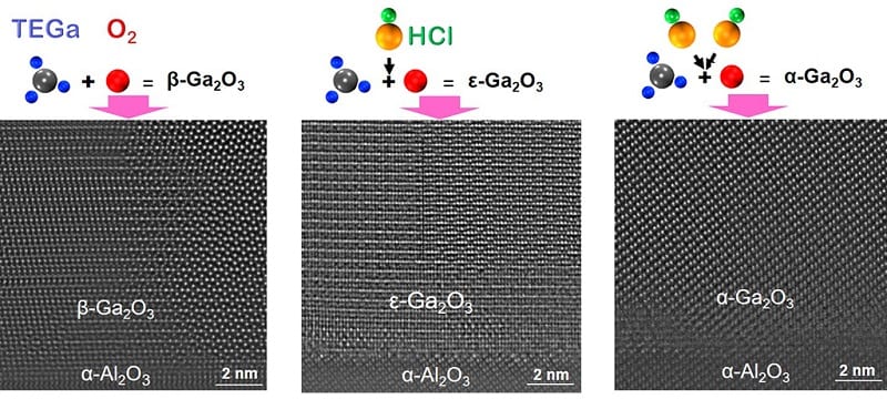
The atoms in gallium oxide can be arranged in a number of different forms known as polymorphs. β‑Ga2O3 is the most stable polymorph but is difficult to grow on substrates of other materials. ε‑Ga2O3 has been grown on sapphire but its growth rate has been difficult to control.
Different polymorphs of gallium oxide can be grown in a MOCVD chamber by controlling the flow of hydrogen chloride.
 Different polymorphs of gallium oxide can be grown in a MOCVD chamber by controlling the flow of hydrogen chloride. © Reproduced with permission from reference 1 © 2018 American Chemical Society (click on image to enlarge)
Led by Li, Sun and the team show that they can achieve precise control of the growth rate by adding hydrogen chloride gas to triethylgallium and oxygen in their MOCVD chamber. When they added the hydrogen chloride at a low flow rate, β‑Ga2O3 formed on the sapphire substrate. But as they increased the flow rate, they were able to create ε‑Ga2O3 and even α‑Ga2O3.
"We are now using kinetic models to unveil the whole mechanism of the crystallization process when hydrogen chloride is used," says Sun, "while also working on fabricating transistors using the three phases of gallium oxide films."
KAUST have begun a close collaboration with Semiconductor Manufacturing International Corporation, an integrated-circuit foundry that provides semiconductor technology services, to fulfill its mission to pursue gallium-oxide semiconductors for practical power-electronic applications.