Facebook
 Google
 GitHub
 Linkedin
Transphorm Announces 185 Million Contract from Office of Naval Research to Establish Domestic Source of Gallium Nitride Epiwafers
This article features Transphorm Incorporated announcement of N68335-19-C-0107 contract with U.S. Department of Defense (DoD) Office of Naval Research (ONR)
Project to Produce First Commercialized Nitrogen Polar GaN for RF/mm-wave for DoD/5G
Transphorm Inc.—the leader in the design and manufacturing of the highest reliability high-voltage (HV) Gallium Nitride (GaN) semiconductors—today announced that the U.S. Department of Defense (DoD) Office of Naval Research (ONR) has exercised a three-year $15.9 million option on an existing $2.6 million base contract with the company. This contract, N68335-19-C-0107, administered by Naval Air Warfare Center Aircraft Division, Lakehurst establishes Transphorm as a U.S.-based dedicated production source and supplier of GaN epiwafers for DoD and Commercial radio frequency (RF)/millimeter wave (mm-wave) and power electronics applications. The award comprises a Base Program for key technology development/transfer and an Option Program to establish production scale capability.
The program’s core objective is to commercialize nitrogen polar (N-polar) GaN, a breakthrough technology beyond the incumbent Ga-polar GaN. N-polar GaN holds significant promise for the continued advancement of GaN-based electronics, in today’s RF electronics and future power conversion systems. The technology, exclusively licensed to Transphorm, was invented under ONR and DARPA sponsorship at the University of California, Santa Barbara (UCSB) by the team of Professor Umesh Mishra, Distinguished Professor at UCSB and Transphorm’s Co-founder, CTO and Chairman.
“The N-polar orientation of the material is reversed from the traditional Ga-polar GaN currently being widely used in base station and DoD applications. The flip produces radical benefits in output power along with groundbreaking efficiencies to frequencies as high as 94 GHz,” said Dr. Mishra. “Applications span the frequency range of interest for 5G, 6G and beyond and also fill a critical technological void for DoD systems.”
At 94 GHz, Mishra’s UCSB team has demonstrated mm-wave devices with record power densities and high efficiencies. These devices simplify RF electronic systems by reducing the need for power combining multiple components and devices while also simplifying cooling systems, ultimately resulting in higher performance at reduced cost.
Leveraging Transphorm’s Well-established MOCVD/GaN Epi Capability
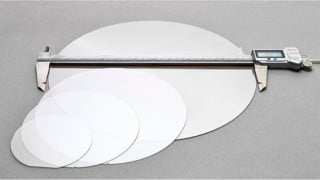
Currently in production with several customers, Transphorm stands as a leading supplier of high quality, high reliability (Q+R) HV GaN FETs. The company’s success is driven by a vertically-integrated business approach, expertise, IP, and, particularly, a solid MOCVD epi growth platform with production scale. With this ONR program, the company will address epi capability on multiple platforms including SiC, Si, and Sapphire substrates ranging from 4-inch to 6-inch and ultimately 8-inch wafers. In the RF and mm-wave area, Transphorm will be a pure play epiwafer supplier focused solely on GaN materials.
“We are excited to partner with the ONR and DoD to commercialize our high performance GaN HEMT IP and epitaxy capability, specifically via the breakthrough N-polar and Ga-polar materials on various substrates including Silicon Carbide, Sapphire, and Silicon,” said Primit Parikh, Co-founder and COO, Transphorm. “This enables Transphorm to grow an adjacent vertical, that of epiwafer sales for DoD customers and fast-growing RF/5G markets. We are already seeing demand and are excited to go from purchase to production in less than 36 months, a key program goal.”
As with all Transphorm GaN products, the epiwafer offerings will be backed by:
- Rapid development
- Production scalability
- Uniform, high yielding wafer products
- Statistical Process Control manufacturing
Availability
Epiwafer inquiries should be directed to Dr. Ron Birkhahn, Director MOCVD, Transphorm ([email protected]).
Design Resources and Support
- Ga-polar and N-polar GaN baseline processes on multiple substrates of various diameters
- Comprehensive suite of GaN epiwafer characterization equipment
- MOCVD experts to align on specific customer requirements
Welcome to the GaN Revolution!
Transphorm designs and manufactures the highest performance, highest reliability 650 V and 900 V GaN semiconductors for high-voltage power conversion applications. Holding the largest IP portfolio (1000+ issued and pending patents worldwide), Transphorm produces the industry’s first JEDEC and AEC-Q101 qualified GaN FETs. This is due to a vertically-integrated business approach, which allows for innovation at every development stage: design, fabrication, device, and application support. Transphorm: moving power electronics beyond Silicon limits.
About Transphorm
Transphorm is a global semiconductor company, leading the GaN Revolution with the highest performance, highest reliability GaN devices for high voltage power conversion applications. To ensure this, Transphorm deploys its unique vertically-integrated business approach that leverages the industry’s most experienced GaN engineering team at every development stage: design, fabrication, device and application support. This approach, backed by one of the industry’s largest IP portfolios with over 1000 patents, has yielded the industry’s only JEDEC- and AEC-Q101-qualified GaN FETs. Transphorm’s innovations are moving power electronics beyond the limitations of silicon to achieve over 99% efficiency, 40% more power density and 20% lower system cost—and here’s how we do it.
Transphorm is dedicated to educating and supporting customers developing with high voltage GaN. Let us know how we can help you!