Facebook
 Google
 GitHub
 Linkedin
Power MOSFET Designs Target Specific Application Needs
Nexperia, Toshiba, and Infineon have designed MOSFETs that offer different strategies in advancing high-power design.
Nexperia, Toshiba, and Infineon have each introduced new additions to their power MOSFET portfolios, with releases spanning application-specific enhancements, process technology updates, and packaging innovations. These upgrades provide transparency into how different power semiconductor vendors are pursuing distinct designs to meet priorities and strategies across the industry.

Toshiba, Nexperia, and Infineon have introduced new MOSFETs. Image used courtesy of Toshiba
Nexperia’s ASFETs with Tighter Dynamic Current Sharing Control
Nexperia has added two application-specific FETs (PSMN1R9-80SSJ and PSMN2R3-100SSJ) into its portfolio. The new MOSFETs feature withstand voltages of 80 V and 100 V, with channel resistances of 1.9 mΩ and 2.3 mΩ, respectively. Given these specs, they are marketed toward 48 V power systems requiring parallel operation, including applications such as forklift motor drives, mobility devices, and high-power industrial motors.

The ASFETs from Nexperia. Image used courtesy of Nexperia
The devices improve dynamic current sharing when multiple MOSFETs are connected in parallel. Nexperia cites up to 50% lower current imbalance during transients, along with a narrower VGS(th) spread of ~0.6 V. With continuous drain current ratings up to 255 A, avalanche ruggedness, and 175°C operation, the aim is improved reliability in systems where fast transient events can otherwise lead to uneven conduction and premature device stress.
Toshiba’s U-MOS11-H Process Pushes 100 V Boundary
Toshiba has launched the TPH2R70AR5, a 100 V N-channel MOSFET based on its U-MOS11-H process technology. Notable performance metrics include an on-resistance of 2.7 mΩ, an improvement of roughly 8% compared to prior devices, and a 37% reduction in total gate charge (Qg). Given this resultant reduction in conduction and switching losses, Toshiba is offering the devices for use in switched-mode power supplies in industrial environments.
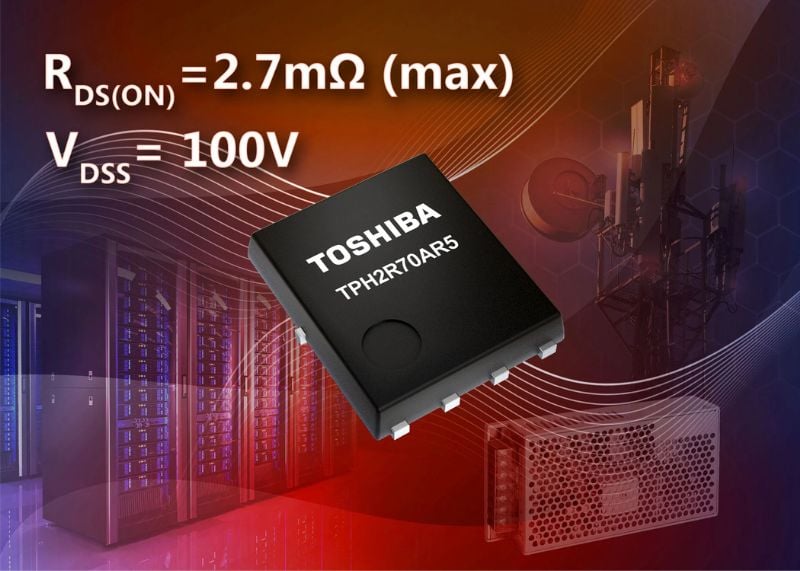
Toshiba’s 100 V N-channel FET. Image used courtesy of Toshiba
Similarly, the R·Qg figure of merit improves by 42%, and the reverse recovery charge is reduced by 38% for quieter operation with fewer voltage overshoots. Thermal handling extends to junction temperatures of 175°C, with current ratings of up to 190A at 25°C.
Infineon’s CoolSiC G2 Extends to 400-440 V
Infineon expanded its CoolSiC MOSFET Generation 2 portfolio with additional 400 V devices in top-side-cooled TOLT, TO-247-3, TO-247-4, and TOLL packages, plus three new 440 V continuous (455 V transient) MOSFETs in TOLL.
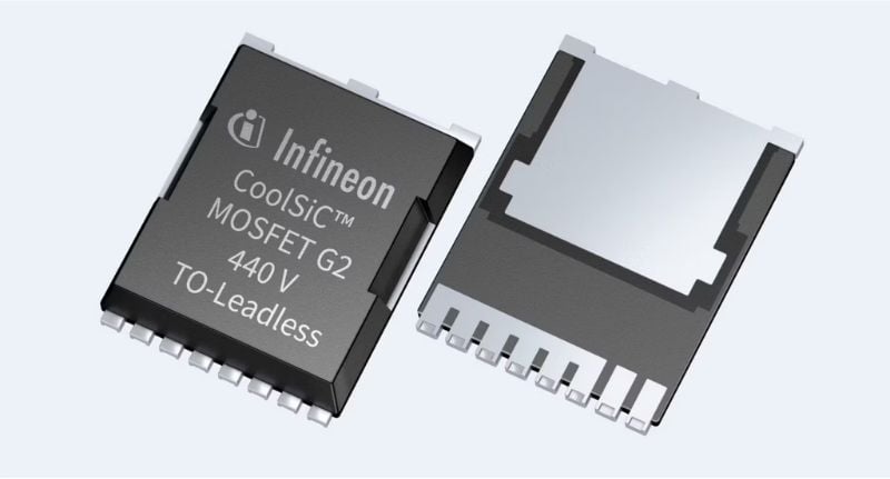
Infineon’s new top-side-cooled devices. Image used courtesy of Infineon
The SiC devices aim to deliver lower conduction losses with flatter RDS(on) vs temperature behavior and up to 50% lower losses compared to silicon MOSFETs at elevated junction temperatures. Reverse recovery charge is reduced by a factor of five or more versus silicon, and system-level testing in totem-pole PFC converters shows peak efficiency improvements of ~0.4 percentage points and up to 15% lower total losses compared to advanced silicon designs.
Infineon also boasts that the device’s packaging flexibility, including top-side cooling and multi-lead layouts, enhances thermal dissipation and layout optimization, giving designers more freedom to balance efficiency and power density.
Infineon’s Application-Optimized OptiMOS 7
Infineon also extended its automotive lineup by introducing the OptiMOS 7 family. Within the family, the MOSFETs are uniquely segmented into variants optimized specifically for high-speed switching, motor-drive efficiency, or ultra-low RDS(on) operation.
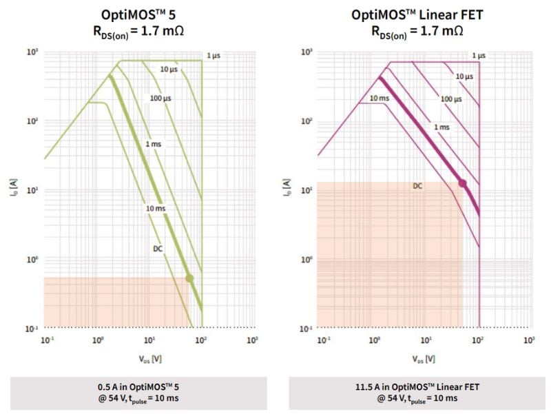
The OptiMOS 7 family. Image used courtesy of Infineon
Compared with the earlier OptiMOS 5 family, the OptiMOS 7 line delivers a 20 to 25% improvement across several performance benchmarks. Devices tailored for high-speed switching provide a better balance between the Miller ratio and the RDS(on)-Qg tradeoff, making them well-suited for hard-switching circuits. Versions aimed at motor-drive applications emphasize reliability by offering a safe operating area up to three times wider than previous generations. For designs where conduction losses dominate, low-RDS(on) options reduce resistive losses and improve overall efficiency under heavy current loads.
Infineon also claims construction-level improvements, such as copper clip interconnects, thin wafers, and advanced packaging that reduces parasitics to improve thermal and electrical performance. Package formats include source-down PQFN for compact switching devices and SuperSO8/PQFN for motor drive parts.
Different Paths in Power MOSFET Development
Between application-specific tuning, process-based efficiency gains, and packaging enhancements for thermal management, the latest announcements show three complementary paths in MOSFET development. While each approach tackles a different system design bottleneck, they all converge on higher density goals, improved conversion efficiency, and long-term reliability.