Facebook
 Google
 GitHub
 Linkedin
Onsemi Unveils Platform That Turns Silicon Wafers Into Power Packages
By embedding heterogeneous Si, SiC, and GaN die directly into 12-inch silicon wafers with precision RDLs, Onsemi's EPP replaces wire bonds and mold compounds to deliver up to 5x power density.
Today, Onsemi introduced its Embedded Power Platform (EPP). Rather than housing power transistors in conventional plastic or ceramic packages, EPP brings packaging into the 12-inch silicon wafer fabrication environment, using the silicon wafer itself as the package foundation.
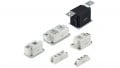
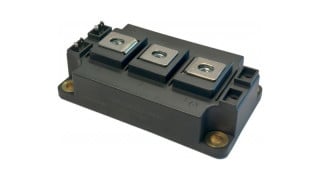
As high-density AI data center racks, electric vehicle (EV) powertrains, and industrial automation systems demand increasingly higher power levels in tighter spaces, traditional power electronic packaging is reaching its physical limits. For decades, power systems have relied on a sequential development model: semiconductor dies are fabricated, mounted onto insulated substrates, wire-bonded, and encased in mold compounds.
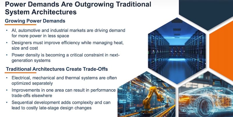
New demands and complexities are driving a need for a new approach to power architectures.
Electrical, thermal, and mechanical systems are optimized separately, forcing engineers to make late-stage design trade-offs that increase system volume, elevate parasitic losses, and extend development cycles. The new platform is aimed at overcoming these challenges.
In order to learn more about this news, we were pleased to talk with Allyson Fairchild, Strategic Project Lead - Corporate Strategy and Advanced Projects at Onsemi.
“A new approach is necessary in order to create a power-dense system and try to manage some of the tradeoffs that we have in the current traditional architectures” said Fairchild. “Higher power density is going to require that these systems are optimized together. And we need to avoid some of the complexity and late-stage design changes that happen with sequential development today.
Rethinking Packaging: The Wafer as the Architecture
EPP transforms the package from a passive housing into an active performance enabler. By performing critical assembly steps directly inside a controlled semiconductor fab, Onsemi applies cleanroom fabrication precision to power system integration.
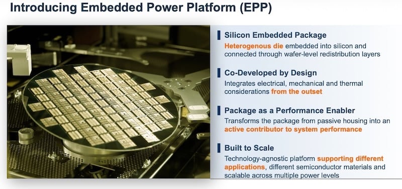
EEP rethinks the package as an active performance enabler rather than just a passive housing.
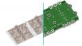
Instead of routing power through long, inductive wire-bond traces, EPP embeds heterogeneous power die directly into cavities within a 12-inch silicon wafer. Embedded devices are interconnected using precisely patterned, wafer-level copper redistribution layers (RDLs) and vertical vias.
“What's really interesting about this is that we're taking our bread and butter as a semiconductor company and what we do best every day, which is fabricating silicon wafers, and we are taking advantage of that and moving it into the high-power space,” said Fairchild. “The package then becomes a performance enabler.”
Key structural aspects of the platform include:
- Heterogeneous Material Compatibility: Supports combinations of Silicon (Si), Silicon Carbide (SiC), and Gallium Nitride (GaN) die alongside low-voltage silicon controllers, gate drivers, and microcontrollers within a single wafer structure.
- Elimination of Wire Bonds: Precision copper RDLs replace wire-bond interconnects, drastically minimizing parasitic inductance and electrical path lengths.
- Configurable Topology: Enables parallel die layouts to reduce RDSon, as well as integrated half-bridge topologies, gate loops, and power stages within one module.
Co-Optimizing Electrical and Thermal Performance
By shifting interconnects to wafer-level processing, EPP enables tighter electrical coupling between power transistors and their driver circuits. This short, controlled electrical path is particularly beneficial for fast-switching wide-bandgap materials like GaN, where parasitic gate inductance normally hinders high-frequency operation. Tighter gate loops allow for higher switching frequencies, improved control, and reduced switching losses.
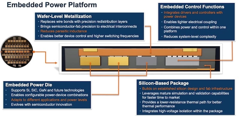
EEP’s wafer-level approach offers advantages such as reduced parasitic inductance and ability to integrate drivers and controllers.
Thermally, EPP leverages the intrinsic properties of silicon. While traditional epoxy mold compounds act as thermal insulators, silicon exhibits high thermal conductivity. Heat generated by the embedded die can conduct across the full footprint of the silicon package directly to external cold plates or liquid cooling systems.
Furthermore, high-voltage dielectric isolation is integrated directly into the silicon structure during fab processing. This replaces thick, thermally resistive Direct Bonded Copper (DBC) or Active Metal Brazing (AMB) substrates with a dense, non-porous isolation layer, maintaining high breakdown voltages without sacrificing heat transfer.
“What we're doing is embedding power dies into a silicon wafer,” said Fairchild. “We're supporting all power technology today: silicon, silicon carbide, gallium nitride. But we're agnostic, so we also can take a look at future technologies when the time comes. We're enabling configurable power device combinations. So in one module, we can look at things like multiple die in parallel to reduce RDSon. We can configure this as a half-bridge, we can add a controller or a gate driver.”
“We can really adapt to different applications. And we can change the types of power die and adapt to different power levels."
System-Level Impact: AI Data Centers and Electrification
The co-optimization of electrical, thermal, and mechanical characteristics delivers measurable space and efficiency gains across target markets:
- AI Data Center Infrastructure: In high-density server racks where power delivery modules compete with compute hardware for space, EPP power designs achieve up to a 30% reduction in footprint compared to sampling solutions while increasing the effective thermal conduction area. In solid-state circuit breaker prototypes, EPP reduced overall system volume by roughly 50% while operating 20% cooler.
- Electric Vehicles (EVs): Applied to traction inverters, EPP offers up to 4x higher power density and up to 15% lower power losses than conventional packaging. A single, scalable EPP power stage architecture can span multiple vehicle power classes, enabling automakers to reuse unified designs across low-end and high-end vehicle lines.
- Development Velocity: By pairing fab-level manufacturing precision with multiphysics digital twin simulation, engineering teams can co-simulate electrical, thermal, and mechanical parameters concurrently in software. This reduces the need for physical hardware iterations, slashing development timelines to as little as four months.
Market Timeline and Early Partners
Automotive manufacturer Subaru has signed on as an early engagement partner for EPP, collaborating with Onsemi to evaluate the platform for next-generation electrified vehicle powertrains. Early access includes engineering samples, simulation models, and technical support to explore efficiency and space improvements in future EV platforms.
Onsemi says it plans to begin shipping early EPP engineering samples to strategic automotive and AI ecosystem partners in 2026.
All images used courtesy of Onsemi.