 Facebook
 Google
 GitHub
 Linkedin
Maxim Integrated’s Newest PMIC Shares One Inductor Across four Buck-Boost Channels
The new SIMO power management IC (PMIC) is said to cut solution size by 70% for ultra-portable wearables.
The MAX77655 is a single inductor multiple-output (SIMO) power management IC (PMIC) that distributes 700 mA from one inductor to 4 independently programmable buck-boost converters. The device takes up only 3.95 mm2 of board space, provides up to 90% regulator efficiency at moderate or heavy demand. The unit draws as little as 6.0µA of quiescent current, and the shutdown current is 0.3µA

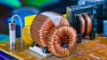
The MAX77655. Image courtesy of Maxim Integrated
What is a SIMO?
SIMO (single inductor multiple output) converters consist of multiple buck-boost converters in a single tiny package that share one inductor. It employs a specialized controller that manages the current flow from the inductor, as needed, to each converter.
This solution still allows each individual buck-boost to be independently programmed to provide each of the separate voltage rails that an OEM design may call for.
The inductor is generally the physically largest component of a wearable device’s power conversion system. By replacing multiple inductors with only one, one of the many benefits of SIMO architecture is the great savings in size that can be achieved.
Maximum Battery Life and Minimum Form Factor
“The MAX77655 breakthrough SIMO topology ushers in new capabilities to millions of small, battery-operated and cloud-connected systems. The highest power density that this solution offers opens avenues for wearables and AI edge manufacturers, whose vision is to boost the 'intelligence quotient' and data point collection for these devices,” said Karthi Gopalan, director, Mobile Power Business Unit at Maxim Integrated. "Designers can now pack an array of precision sensors with the highest processing power while delivering on the most critical customer need of maximum battery life in the smallest form factor.”
Specifications
The minimum and maximum input voltages are 2.5 and 5.5 VDC, respectively. There are four independent outputs that can each be programmed over a range of 0.5 to 5.5 VDC
A bidirectional I2C bus is used to control the MAX77655 and for status checking. In addition to programming the unit by the I2C bus, various factory programmable options are available. These allow for the device to be tailored by Maxim to customer-specific needs, cutting down on customer design time.

Simplified block diagram for the MAX77655. Image courtesy of Data Sheet
Typical UVLO and OVLO thresholds are 2.3 and 5.85 volts, respectively. Typical junction lockout temperature is 145℃
The MAX77643/MAX77642
Maxim also offers the MAX77642/MAX77643, which are also SIMO PMICs. They accept inputs ranging from 2.7 to 5.5 VDC. Three independently programmed output that can range from 0.5 to 5.5 volts, the total current is 500 mA.
Applications
- True wireless stereo (TWS) Bluetooth
- Fitness and health devices
- Headphones and hearables
- Portable and wearable devices
- Smartwatches
- Commercial and consumer IoT
Physical and Environmental Considerations
- Operating temperature range is from -40 to +85℃
- The MAX77655 is available in a 3.95 mm2 16 bump wafer-level package (WLP/16) with a 0.5mm-Pitch.
- Lead free, RoHS compliant
Getting to Market Faster
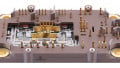
The MAX77655 evaluation kit makes it easy for designers to learn about and evaluate the MAX77655.

Image courtesy of MAX77655 Evaluation Kit Data Sheet
Windows-based software is included to provide a convenient graphical interface in addition to a register-based interface to exercise the features of the MAX77655.


