Facebook
 Google
 GitHub
 Linkedin
EPC Claims its New 350 V GaN Transistor is 20 Times Smaller than Comparable Silicon Offerings
The enhancement mode power transistor features a maximum continuous drain current of 6.3 A and a maximum RDS(ON) of 80 mΩ
Gallium nitride (GaN)-based semiconductors, along with their silicon carbide (SiC) cousins, are continuing their inevitable march toward dominion over the power semiconductor field. Amidst that backdrop, Efficient Power Conversion (EPC) released Thursday its new EPC2050 GaN power transistor, which it says is 20 times smaller than comparable last-generation silicon transistors, and cheaper.
Priced at $3.05 per unit for quantities of 1,000, the device is available in a 1.95 mm2 passiveated die form. Packing that type of punch as a die, rather than in bulkier packages, offers designers significant flexibility.
“With the EPC2050, designers no longer have to choose between size and performance,” said EPC’s CEO, Alex Lidow. “They can have both and [at] lower cost!”

The EPC2050 is available in a 1.95 mm2 die. Image used courtesy of EPC
Though it’s difficult to independently verify EPC’s claims, it does have significant design acumen here. The company has been quite active in the field of tiny enhanced mode transistors. Other recent devices include:
- The EPC2069, a 40 V device with a maximum current of 80 A, on a die sized 3.25 x 3.25 mm
- The EPC2054, a 200 V eGaN FET that handles 3 A continuously and is offered on a 1.69 mm2 die
- The EPC2059, which handles a maximum of 170 V drain-to-source, packaged on a 2.8 x 1.4 mm die
The 120 VAC Americas Market
The EPC2050 is a fast-switching semiconductor, readily suitable for 120 VAC applications. A typical power supply features bus voltage of between 170 V and 250 V, which includes applications specific to the Americas market, including power tools, in-wall powered devices, seat-back airline 120 V inverters, and commercial LED lighting. Other applications that will benefit from the EPC2050’s fast-switching speed and its tiny size include DC-DC conversion from, or to, voltages in the 120 to 160 VDC range.
Maximum ratings
Drain-to-source voltage:
- 350 V continuous
- 420 V pulses. Up to 10,000 5 ms pulses at 150 °C
Drain-to-source current at 25℃
- 6.3 A continuous
- 26 A for 300 µs pulses
Dynamic Characteristics (typical)
- Input capacitance: 423 pF
- Reverse transfer capacitance: 0.3 pF
- Output capacitance: 81 pF
- Gate resistance: 0.5 Ω
- Total gate charge: 2.9 nC
- Gate-to-source charge: 1.3 nC
- Gate-to-drain charge: 0.3 nC
- Gate charge at threshold: 0.9 nC
- Output charge: 35 nC
- Source drain recovery charge: 0 nC
Applications
- Aerospace
- Control of 120 to 150 V medical motors
- Multi-level converters such as Totem Pole PFCs
- Fast chargers
- Battery management systems (BMS)
- Solar power inverters
- High-power LIDAR
- LED lighting
- RF switches
- Class D audio
- Medical imaging
Physical Considerations
- The EPC2050 operates over a junction temperature range of -40 to 150 ℃.
Environmental Notes
- RoHS-compliant
- Halogen-free
Getting to Market Faster
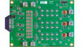
EPC offers the EPC90121 development board to help designers quickly familiarize themselves with the EPC2050.

Front (left) and back (right) views of the EPC90121. Screenshot used courtesy of EPC
The board measures 2 by 2 inches, features two EPC2050s in a half bridge configuration, and employs the onsemi NCP51820 gate driver. Maximum device voltage is 350 V, and maximum output current is 4 A. The board offers multiple probe points to facilitate simple waveform measurement and efficiency calculations.
Feature image used courtesy of EPC
Related Content