Facebook
 Google
 GitHub
 Linkedin
Efficient Power Conversion (EPC) Debuts a 1.6 mΩ, 40 V eGaN FET
The new enhancement mode power transistor features a maximum ID of 80 amps with a die size of only 3.25 x 3.25mm.
EPC touts the EPC2069 as being suitable for high power density performance applications such as 48V – 54V input servers.

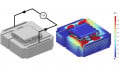
The EPC2069. Image courtesy of EPC
As described in the announcement, the EPC2069 is said to be applicable to use cases presenting tough requirements for high power density performance including 48 V – 54 V input servers. This enhancement mode power FET offers zero reverse recovery losses and low gate charges allowing for high-frequency operation at 1 MHz and better.
With a footprint of only 10.6 mm2, the unit can support high-density, state-of-the-art high applications ranging from 500 W to 2 kW and with efficiencies upward of 98%. Through the use of eGaN devices in both the primary side and the secondary side of power converters, EPC contends that maximum power densities greater than 4000 W/in3 are achievable.
Major Use Cases for the EPC2069
According to Alex Lidow, EPC’s co-founder and CEO, “The EPC2069 is perfectly designed for the secondary side of the LLC DC-DC converter from 40 V – 60 V to 12 V, which is becoming very common for the new 48 V – 54 V input servers required for high density computing applications such as artificial intelligence and gaming. This 40-volt device offers both smaller size and reduced parasitics compared with previous-generation 40 V GaN FETs and at lower cost; thus, offering designers both improved performance and cost savings.”
Complete information on the EPC2069 can be found in the datasheet
Maximum Ratings
- Continuous drain-to-source voltage is 40V, and the unit can sustain up to 10,000 5ms pulses of 48V at 150℃.
- Continuous drain-to-source current is 80A, and 300µs pulses of 422A can also be tolerated.
- Maximum Gate-to-Source Voltages are +6V and -4V
Thermal Resistances
Typical values are:
- Junction-to-Case: 0.35 °C/W
- Junction-to-Board: 1.1 °C/W
- Junction-to-Ambient: 46 °C/W
Dynamic Characteristics
At TJ of 25℃, typical values are:
- Input capacitance: 1351pF
- Reverse transfer capacitance: 32pF
- Output capacitance: 1044
- Total gate charge (QG): 12.5nC
- Gate-to source charge: 3.9nC
- Gate-to-drain charge: 2.4nC
- Output charge: 32nC
- Gate resistance: 0.4Ω
Physical Considerations
- The EPC2969 is available in passivated die form, die size is 3.25 x 3.25mm
- The unit operates over a temperature range of -40 to 150℃
Applications
- DC-DC Converters
- BLDC Motor Drives
- Sync Rectification for AC/DC and DC-DC
- Lidar/Pulsed Power
- Class-D Audio
- LED Lighting
Environmental Considerations
- RoHS compliant
- Halogen-free
Getting to Market Faster
The EPC90139 is a Development Board for the EPC90139. Measuring 2 x 2 inches, it contains two EPC2069 GaN FET in a 40 volt half-bridge configuration.

Block diagram of the EPC90139 development board. Image courtesy of Quick Start Guide
The development board serves to make it simpler for engineers to simplify the process of evaluating the EPC2069. The board contains all the necessary components on a compact board and is applicable to most existing converter topologies.