Facebook
 Google
 GitHub
 Linkedin
Easy Design of 1500 VDC Renewable Inverter With Higher Power Density Enabled by New 2.0 kV Class LV100 IGBT Module
The 2.0 kV module is offering a competitive solution due to its simplified inverter design and layout, higher power density and high level of scalability.
Using 1700 V IGBT power modules for 1500 VDC applications carries many risks for unpredicted converter failures. Instead, a newly developed 2.0 kV Class IGBT module is enabling a reliable and efficient usage of simple 2-level topology for 1500VDC renewable inverter systems.
Conventionally available IGBTs with 1700 V blocking voltage are designed for the requirements of motor control applications in 690 VAC networks where DC-link voltage is typically about 970 V and maximum below 1200 V. For renewable applications, higher DClink voltage is required going up to 1500 V which is the limit of the low voltage directive (2014/35/EU). Hence, a new 2.0 kV class IGBT in the LV100 housing has been developed and evaluated under the requirements of renewable applications such as photovoltaic and wind energy converters. The new 2.0 kV class IGBT solution has been compared with available options like 1700 V class IGBT or 1200 V class IGBTs in a 3-level NPC topology regarding power losses, operation temperatures, power density, mechanical design constraints and long-term DC bias stability (LTDS).
Background of 2.0 kV IGBT Development
In recent years, a DC-voltage of 1500 V has become the standard for utility-scale photovoltaic power plants. PV panel oversizing is pushing the MPP (maximum power point) voltages and even continuous operation up to 1400 V for central PV inverters [1]. In wind converters with classical 690 VAC voltage, DC-link voltage of more than 1200 VDC is required considering reactive power demand [2]. In addition, grid events such as high-voltage ride through can cause higher short term DC-link voltages. Also, higher wind converter output voltages such as, e.g. 900 VAC are considered to enable systemcost reduction [1]. Hence, in wind converters, the voltages come closer to the low voltage directive border of 1500 VDC / 1000 VAC. A similar trend is in battery energy storage system application. Due to the limitation of 1700 V class IGBTs under such operating conditions, a new 2.0 kV class IGBT is required to enable a reliable operation of a 2-level topology inverter at the required DC-link voltages.
The LV100 power module package has been selected to implement the new 2.0 kV chipset to fulfil the requirements of high power renewable converter systems for high current ratings and superior power density [3].
Limitation of 1700 V Power Modules
1700 V is an established voltage class for IGBT power modules - particularly because they are well suited for 690 VAC systems which are frequently used for high-power industrial applications. However, in case of usage for 1500 VDC application, there are high risks why 1700 V IGBT should not be used.
A well-known and understood failure mechanism is the spontaneous failure due to cosmic rays. It refers to particles, which results from cosmic radiation and the penetration with the Earth’s atmosphere, interfere with the semiconductor in power modules. With a certain probability, this interference could cause the semiconductor to fail. It is important to notice, that the cosmic ray failure is a random failure which can occur anytime with a certain probability. This probability is constant over lifetime, different from a wear-out failure whose failure probability increases with increasing operating time of the power module.
The probability for cosmic ray failures depends mainly on the power module’s voltage class and the applied voltage. The failure probability, or rather the failure rate, is measured in the laboratory and finally expressed as LTDS capability [8]. These measurements show, that the LTDS capability 1700 V power modules is insufficient for 1500 VDC applications. Operation at 1400 V – 1500 V will lead to random field failures with unacceptably high failure rates. This will be discussed further below.
Besides cosmic ray failures, the peak over voltage is another limitation when operating power modules at high DC-link voltage. During turn-off of the power module, a transient over voltage is induced due to the inherent inductances in the main circuit which consist of parasitic stray inductance of power module, busbars and the DC capacitors. This voltage adds up to the DC link voltage. The sum of both, DC link voltage and transient overvoltage, is to be kept always bellow the break down voltage of the semiconductor. It becomes obvious that when a 1700 V IGBT power module is operated at 1500 V, the head room for the over voltage is only 200 V.
This is only technically feasible if severe current derating is considered and switching speed is reduced heavily. Consequently, losses in the semiconductor increase, converter efficiency decreases, and converter output power is to be reduced.
Considering cosmic ray failures and overvoltage derating, it becomes evident that 1700 V class power modules are unsuitable for developing converters with 1500 V DC link. The risk of developing an unreliable, inefficient and overall uncompetitive converter is obvious.
Mitsubishi’s 2.0 kV Power Module
MITSUBISHI ELECTRIC’s solution for converters with up to 1500 V DC-link voltage is a newly developed T-Series 2.0 kV power module. The power module features the latest 7th-generation IGBT and RFC (Relaxed Field at Cathode) diode. Together with the state-of-the-art LV100 package, as shown in Figure 1, the power module offers high power density and simplified parallel-connection. The new 2.0 kV CM1200DW-40T is expanding the comprehensive LV100 and HV100 line-up as shown in table 1.

Figure 1. Newly 2.0 kV power module in the LV100 package. Image used courtesy of Bodo’s Power Systems [PDF]

Table 1. LV100 and HV100 Line-up. Image used courtesy of Bodo’s Power Systems [PDF]
The schematic cross section of IGBT and diode chips is shown in figure 2. The RFC diode structure with lightly, graded doped thin LPT(II) N buffer with a combination of shallow N+ and P layer on the cathode side contribute to the sufficient blocking characteristics of 2.0 kV with low forward voltage. The RFC diode structure allows suppressing the oscillations at high DC-link voltage without scarifying the low Err vs. VF characteristic [7].

Figure 2. Cross section view of 7th generation IGBT chip (left) and RFC diode chip (right). Image used courtesy of Bodo’s Power Systems [PDF]
When increasing blocking voltage capability from 1700 V to 2.0 kV, increasing forward voltage and / or switching energy can be expected. This effect has been investigated thoroughly during the development of the 2.0 kV power module. Figure 3 shows the IGBT forward voltage VCEsat in dependence on the turn-off energy Eoff for different voltage classes. We can see that, while the trade-off curves for different voltage classes are shifted, it was able to maintain for the 2.0 kV module a similar VCEsat as for a 1700 V device. Figure 4 similarly shows the diode’s forward voltage Vf in relation to the reverse recovery energy Err. For the final design of the 2.0 kV power module, a diode with a low forward voltage is selected.

Figure 3. Trade-off characteristics of different voltage class IGBT. Image used courtesy of Bodo’s Power Systems [PDF]

Figure 4. Trade-off characteristics of different voltage class diodes. Image used courtesy of Bodo’s Power Systems [PDF]
As discussed earlier, for 1700 V power modules, long-term DC stability (LTDS) is one of the bottle necks for 1500 V applications. Now, figure 5 shows a comparison of the measured failure rate of 1700 V and the new 2.0 kV device. As measurements show, LTDS capability of the new 2.0 kV device has been improved significantly.

Figure 5. LTDS curves of 1200 A for different voltage class power modules. Image used courtesy of Bodo’s Power Systems [PDF]
Figure 3 to figure 5 demonstrate nicely the tradeoff between power device losses and LTDS capability. We are convinced that the 2.0 kV power module is an efficient, rugged and well-balanced solution for many 1500 VDC applications.
Benchmark With 3-level Topology
As explained, a 2-level topology based on 1700 V IGBTs is considered as not reliable due to insufficient margins and cosmic ray induced failure rates. Conventionally, 3-level (A)-NPC topology based on 1200 V IGBTs is used for 1500 VDC Inverters. This conventional approach has been benchmarked with the novel simplified 2-level solution based on new 2.0 kV Class LV100 IGBT module.
a) Application Conditions
The most popular available solution for inverters with 1500 VDC is a 3-level topology based on 1200 V IGBTs.

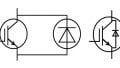
Figure 6. Circuit topologies. Image used courtesy of Bodo’s Power Systems [PDF]
Hence a benchmark and evaluation has been carried out by comparing the 3-level topology based on 3 pcs 1200 A/ 1200 V type LV100 modules CM1200DW-24T with the 2.0 kV CM1200DW-40T in a 3-times parallel configuration. The nominal limit of DC-link voltage is determined by the low-voltage directive with VDC=1500 V. For continuous operation, a slightly lower voltage of VDC=1400 V has been selected for the power loss evaluation. As cooling method, a liquid-cooled sink has been assumed, which is state of the art for wind converter systems. A power factor of 1 and a switching frequency of 2.5 kHz have been selected, which are typical values for central PV and grid side wind converter inverter units. For the 3-level solution has been the half switching frequency of 1.25 kHz because of same current ripple considering the comparable filter inductance values. The detailed operating conditions are explained in table 2.
b) Power Loss and Thermal Performance
Under those conditions the losses and temperatures have been evaluated. The result is shown in Figure 7. It can be noticed that the maximum junction temperature of the 1200 A / 2.0 kV LV100 sample (CM1200DW-40T) is 129°C, well below the limitations of Tvjop=150 °C and Tvjmax=175 °C. For the 1200 A / 1200 V modules in the 3-level NPC configuration, the same cooler performance has been considered. However, the maximum junction temperatures reach 145°C, which is close to the specified temperature limits. The background is that in the 3-level NPC topology the losses are concentrated to some of the semiconductor devices. The outer IGBTs Tr1 and Tr4 operate in a huge duty cycle and have to conduct the whole inverter output current amplitude wherein the 2-level topology the paralleled devices share the current.
| Conditions: |
3-level (A-NPC) |
2-level (3x paralleled) |
| VECS | 1200 V | 2000 V |
| paralleling | - | 3 pcs |
| No. of modules per inverter | 9 (3 x 3) | 9 |
| Pout[kW] | 1800 | 1800 |
| Iout[Arms] | 1212 | |
| Iout[Arms] / Module | 1212 | 404 |
| VCC[V] | 1400 | |
| Vout[Vrms] | 857 | |
| cosΦ | 1 | |
| fc[kHz] | 1.25 | 2.5 |
| modulation method | sinusoidal | |
| modulation index | 1 | |
| fout[Hz] | 50 | |
Table 2. Application conditions

Figure 7. Loss and temperature evaluation result of IGBT and diodes in 2-level 2.0 kV and 3-level 1200 V inverter. Image used courtesy of Bodo’s Power Systems [PDF]
As result, the conduction losses of the IGBTs Tr1 and Tr4 are as high as 827 W. In addition, IGBT Tr1 and Tr4 are also involved in the switching operation and 235 W switching losses must be added. Therefore, the total IGBT losses are 1061 W and about 47% higher than the 2.0 kV IGBT losses in the 2-level configuration. This high loss concentration causes a high-temperature rise of the outer IGBTs in the 3-level topology. The high junction temperature is limiting the total inverter output power performance. Considering a junction temperature limit of 150°C in the 3-level topology, the rms output current must be limited to 1250 A. Whereas in the 2-level topology with the 2.0 kV samples, a 24% higher rms output current of 1500 A is possible.

Figure 8. Maximum junction temperature vs. inverter output current for 2-level (3 pcs paralleled 1200 A/2.0 kV) and 3-level (3 pcs 1200 A/1200 V in (A)-NPC configuration). Image used courtesy of Bodo’s Power Systems [PDF]
c) Switching Frequency
It can be noticed that in the 2-level 2.0 kV topology, which operates at switching frequency of 2.5 kHz, the switching losses are dominant part with 69%. Whereas in the 3-level 1200 V topology, the conduction losses have the major share with 97.6%. Therefore, it has been assumed that the 3-level inverter will be beneficial for higher switching frequency. Accordingly, a simulation has been carried out to compare the junction temperature dependency of the 3-level and 2-level inverters. For a switching frequency range of up to 9 kHz, the 2-level inverter has lower junction temperature. From 0 to 1 kHz the 3-level inverter is limited by the junction temperature of the inner IGBTs Tr2 and Tr3. At power factor cos(φ) = 1, losses and temperatures of Tr2 and Tr3 are independent of switching frequency due to purely conduction losses. For switching frequencies of more than 1 kHz, the outer switches Tr1 and Tr4 limiting thermally the 3-level inverter. In the 2-level inverter and given condition, the IGBTs Tr1 and Tr2 show the highest temperatures. However, due to half switched DC-link voltage in the 3-level inverter the switching frequency can be reduced by 50% to achieve comparable current ripple for same AC output filter inductance value as in the 2-level inverter. Therefore, also this switching frequency reduction has been taken into consideration for the 3-level inverter. The result shows that up to a switching frequency of 3.5 kHz (2-level) and 1.75 kHz (3-level), the 2-level inverter with 2.0 kV class IGBT has lower junction temperature and higher output current capability. For switching frequency above 3.5 kHz (2-level) and 1.75 kHz (3-level) the usage of 3-level inverter is considered as beneficial from temperature point of view. In conclusion, the selection of the best inverter topology depends on switching frequency. By using different modulation methods such as DPWM with lower switching losses, the breakthrough point of 3.5 kHz can be shifted to a higher switching frequency level.

Figure 9. Max. junction temperature vs switching frequency for 3-level and 2-level inverter. The dotted line considers half switching frequency for 3-level topology. Image used courtesy of Bodo’s Power Systems [PDF]
Benefits in Inverter Design
The 2.0 kV class IGBT module in LV100 housing enables to use of simple 2-level topology for inverters with DC-voltages up to 1500 V. By avoiding the more complex 3-level topology, the design can be simplified.
a) Commutation Inductance
The commutation inductances in a 3-level topology tend to be higher, to more than 100 nH [6] since more series-connected devices are involved. Especially commutations between several modules involving higher inductances and causing higher turn-off voltage spikes [6]. In the 2-level topology, a low commutation inductance design using the LV100 package can be easily achieved [3] by using laminated busbar designs.
b) IGBT Gate Driver
To control a 3-level NPC inverter, 4 individual gate driver channels are required per phase leg. Hence, 12 control signals and gate driver channels are required for the total inverter. The ANPC (active neutral point clamp) topology is equipped with 2 additional active IGBT switches per phase at the clamp part. Recently, this A-NPC has become popular because of additional commutation paths which allow a reduction in commutation inductance and sharing of losses of inner switches [6]. However, by this topology, 6 individual gate driver channels are required to drive one 3-level A-NPC phase leg. As a result of a total 3-phase inverter, 18 gate driver channels are required. This is three times higher than the required 6 gate driver channels for a classical 2-level inverter. The required gate driver power per channel for the 2-level inverter is higher because of three paralleled modules. However, savings are expected by reduction of the required number of insulated power supplies, signal insulation components (such as photocoupler, signal transformer or fiber optics) and components to realize protection functions (like short circuit, under-voltage or active clamping). Moreover, the LV100 package is specifically designed for parallel connection of power modules [9].
c) Busbar and Heatsink
Design To realize the 3-level topology, 3 half-bridge modules have to be connected per phase leg. For the interconnection of the modules, additional busbars are required. Also, the DC-busbar must consist of three layers instead of two-layer with a 2-level topology. As result, the busbar construction and module arrangement are more complex in the 3-level topology which can be noticed in Figure 10.
In the 2-level topology the modules can be placed in a simple line. By this simple line arrangement, a water cooler with simple cooling channels underneath the modules and chips chip can be easily achieved. Also, in an air-cooled system, the simple line arrangement is considered as beneficial because homogenous cooling can be achieved for all modules. In the 3-level design, the module placement on the heatsink must be compromised with stray inductance considerations which does not result in a simple line arrangement as shown in figure. 10. Therefore, the cooler design is more complex with risk of inhomogeneous cooling conditions.

Figure 10. Example of module and busbar arrangement incl. driver PCB board. Image used courtesy of Bodo’s Power Systems [PDF]
d) Scalability of Power
The LV100 IGBT module housing concept is designed for parallel operation. In this evaluation, a paralleling of three modules has been considered with an achieved output power of 1800 kW. This result in a power of 600 kW per module. By selecting the number of modules, the output power can be easily adjusted in 600 kW steps to the actual application requirement. Therefore the 2.0 kV IGBT in the 2-level inverter providing a high level of scalability. In the 3-level inverter a parallel configuration is considered as difficult because paralleled modules resulting in wider switches and distances in external commutation loops which causing higher commutation inductances. The power step size by paralleling is with 1800 kW three times larger than 600 kW in the 2-level system. Therefore, it is not possible to scale the output power to intermediate values economically.
Summary
It has been demonstrated that the new CM1200DW-40T 1200 A / 2.0 kV LV100 Module is enabling a power density increase of 24% for 1500 VDC renewable inverter systems compared to a 3-level (A)- NPC inverter. Furthermore, several benefits like inverter design simplification, low stray inductance, reduced number of gate driver channels and high level of scalability become available by utilization of 2-level topology with 2.0 kV IGBT modules for 1500 VDC inverters. The power loss, LTDS and thermal characteristics of an 1200 A / 2.0 kV IGBT module in the LV100 package (CM1200DW40T) has been analyzed and compared with 1200 A / 1200 V modules (CM1200DW-24T) in a 3-level configuration. The comparison was done under typical conditions of 1500 VDC inverter for renewable application. By the homogeneous distributed power losses in a 2-level inverter using 2.0 kV power module, the output and power density can be increased by 24% compared to the 3-level NPC inverter where power losses are unequally distributed between IGBTs and are mainly generated in the outer IGBTs.
This article originally appeared in Bodo’s Power Systems [PDF] magazine.