Facebook
 Google
 GitHub
 Linkedin
Consumer Drive Applications – Energy Efficiency and Power Density in SiC Power Devices
Over the past decades, energy regulations have been consolidated highlighting the importance of manufacturing energy efficient products. This has led to saving considerable amounts of energy [1]. Additionally, these directives have paved the way for designing more innovative appliances by utilizing new technologies such as SiC MOSFETs due to their superior intrinsic properties [2]. Adopting such technologies helps manufacturers target the highest energy class label.
Recently, a newly developed advanced integrated power device (IPD), IM105-M6Q1B, was introduced. IM105-M6Q1B offers the benefits of Infineon’s CoolSiC technology and an industry-benchmarked, high-voltage, rugged-driver integrated circuit (IC) in a small 7 mm x 7 mm quad flat no-lead (QFN) package. Using this IPD enables the designing of low-power drives with superior power density as well as extending the output power limits of heat sink-less operation.
A test vehicle drive board was designed, as shown in Figure 1, to test the capabilities of IM105-M6Q1B under typical fridge compressor loading conditions. The block diagram of IM105-M6Q1B is also included in the image. The IPD is composed of a SiC MOSFET half-bridge with a typical on-state resistance of 257 mΩ at Vgs = 18 V and Tj = 25°C and a gate driver based on the silicon-on-insulator (SOI) technology. The maximum blocking voltage has been upgraded to 650 V compared to 600 V in standard devices, offering an additional margin in case of grid voltage fluctuations. Advantages of Infineon’s SOI technology in gate drivers are high switching frequency functionality [3], low ohmic (30 Ω) monolithically integrated bootstrap diode [3, 4], and robust negative transient immunity due to inductive load switching events [5]. Additionally, this gate driver provides fixed internal dead time, typically 540 ns, which is automatically inserted whenever the external dead time is shorter to ensure shoot-through protection. All these gate driver features, together with Infineon’s CoolSiC technology advantages, are offered in a small surface-mounted device (SMD) package.

Figure 1. Drive board test vehicle and block diagram of IM105-M6Q1B. Image used courtesy of Bodo’s Power Systems [PDF]
On-State Output Characteristics
In this section, typical output characteristics of IM105-M6Q1B are discussed at two gate-biased voltages – 15 V and 18 V. In low-power consumer drives market, two commonly employed products are IKD04N60RC2 and IPD60R280PFD7S. In this section, their output characteristics have also been compared with that of IM105-M6Q1B.
The first output characteristic graph is shown in Figure 2. It can be seen that in the first quadrant operation, the voltage drop of IM105-M6Q1B is significantly lower (about 4 A) than that of IKD04N60RC2.
Moreover, the temperature dependency of IM105-M6Q1B on its RDS(on) is, typically, just 0.11 mΩ/°C at Vgs = 15 V and slightly higher, which is 0.2 mΩ/°C, at Vgs = 18 V. This highlights the minor temperature dependency characteristics of the CoolSiC technology. On the other hand, in the third quadrant operation during the conduction time interval of the diode, the voltage drop is higher for IM105-M6Q1B than for IKD04N60RC2. However, note that the diode only conducts during the dead time, which is roughly between 0.5 and 1 µs under application conditions, and therefore, its loss contribution is insignificant. When the SiC MOSFET channel conducts in the third quadrant operation, the voltage drop is slightly lower than the one in the first quadrant operation.

Figure 2. On-state output characteristics of IM105-M6Q1B against IKD04N60RC2. Image used courtesy of Bodo’s Power Systems [PDF]
The second comparison graph is shown in Figure 3. It is evident that the voltage drop of IPD60R280PFD7S in the first quadrant operation at Tj = 25°C is lower than that of IM105-M6Q1B. The typical RDS(on) of IPD60R280PFD7S is 233 mΩ at Vgs = 10 V and Tj = 25°C. For this device type, the increase of the gate bias does not provide an additional reduction in voltage drop, as can be seen in its datasheet. Apart from this, it can also be discerned that the voltage drop temperature dependency of IPD60R280PFD7S is significantly higher than that of IM105-M6Q1B. The typical RDS(on) temperature dependency of IPD60R280PFD7S is approximately 2.53 mΩ/°C and higher conduction losses at elevated junction temperatures than IM105-M6Q1B are expected. Likewise, IPD60R280PFD7S exhibits a lower voltage drop for the forward-biased diode than IM105-M6Q1B.

Figure 3. On-state output characteristics of IM105-M6Q1B against IPD60R280PFD7S. Image used courtesy of Bodo’s Power Systems [PDF]
Finally, the total typical dynamic losses of the aforementioned devices are shown in Figure 4, as derived using a typical double-pulse test setup. Please note that reverse recovery losses were excluded from this analysis because their contribution to the total sum is relatively minor. The voltage rate of change, dv/dt, for both the devices were tuned to be similar at roughly 6.5 – 7 V/ns to ensure a fair comparison. The switching speed of IM105-M6Q1B was tuned internally by its integrated gate driver to be between 6 and 7 V/ns (20 – 80%).
IM105-M6Q1B shows significantly lower energy losses when compared to IKD04N60RC2 and particularly IPD60R280PFD7S, the energy losses of which are dominated by turn-on losses. Last but not least, the dynamic losses of IM105-M6Q1B present negligible dependency on temperature, while in other devices, even at Tj = 100°C, the losses start increasing considerably.

Figure 4. Sum of the turn-on and turn-off dynamic losses at different switching currents and temperatures. Image used courtesy of Bodo’s Power Systems [PDF]
Typical Fridge Compressor Simulation Analysis
A typical fridge compressor presents several operating points throughout its total cycle. The two most distinctive ones are the rated operating point at which the output power is about 40 W and the high load operation in which the output power is roughly 160 W. In this analysis, the PLECS software tool was used to examine the power losses of the three case study devices. The outcome of the simulation, together with typical application conditions, is shown in Figures 5 and 6. The case temperature for these simulations was set to Tc = 110°C. This is, typically, the maximum operating case temperature of a printed circuit board (PCB), as it is limited due to its material properties. At light load or the rated load, IM105-M6Q1B showed almost 43 percent lower losses than IPD60R280PFD7S and 60 percent lower losses than IKD04N60RC2. Under these conditions, increasing the gate voltage to Vgs = 18 V did not provide noticeable benefits.
In the case of high load, IM105-M6Q1B showed almost 37 percent lower losses than IPD60R280PFD7S and 64 percent lower losses than IKD04N60RC2. Here, increasing the gate voltage of IM105-M6Q1B to Vgs = 18 V offered relatively 14 percent lower losses than with the gate voltage Vgs = 15 V, indicating the minimum achievable losses of IM105-M6Q1B.

Figure 5. Split graph of power losses of a typical fridge compressor at given rated conditions. Image used courtesy of Bodo’s Power Systems [PDF]

Figure 6. Split graph of power losses of a typical fridge compressor at given high load conditions. Image used courtesy of Bodo’s Power Systems [PDF]
The efficiency calculation for the inverter stage is given in Table 1. A 2-level, 3-phase inverter was considered in this analysis, i.e., six devices in total. At nominal load, the overall efficiency gain of IM105-M6Q1B was 2.7 percent more than IKD04N60RC2 and almost 1 percent more than IPD60R280PFD7S. At high load conditions, the efficiency gain was roughly 1.5 percent and 0.5 percent against IKD04N60RC2 and IPD60R280PFD7S, respectively.
Table 1. Efficiency calculation of a 6-bridge, 2-level, 3-phase inverter
| Device | Efficiency [%] | |
| Nominal load | High load | |
| IM105-M6Q1B_18 V | 98.77 | 99.29 |
| IM105-M6Q1B_15 V | 98.74 | 99.17 |
| IPD60R280PFD7S | 97.82 | 98.69 |
| IKD04N60RC2 | 96.95 | 97.75 |
Hardware Experiment Results
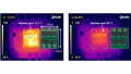
This section discusses additional benefits of IM105-M6Q1B in terms of form factor, i.e., power density. A comparative analysis of the heat sink-less output power capability of similarly designed low-power drive boards with IKD04N60RC2 and IM105-M6Q1B is also provided. Images of the drive boards are shown side by side in Figure 7 to clearly highlight their differences. Both boards include similar electromagnetic interference (EMI) filters, diode rectifiers, DC link capacitors, and the microcontroller IMC101T-T038 (iMOTION IMC100 motor controller).
Both designs have a layout with two copper layers and 35 µm copper traces thickness. The main difference lies in the inverter stage.
The drive board using IKD04N60RC2 requires six discrete IGBTs in a TO-252 package and one full-bridge, 3-phase gate driver IC to form a two-level, 3-phase inverter. On the other hand, the board using IM105-M6Q1B requires significantly less space due to the integration of the half-bridge and gate driver into a QFN package. Consequently, the size of this board can be reduced by 15%, resulting in improved power density.

Figure 7. Low power consumer drives: The blue PCB (left side) uses IM105-M6Q1B, dimensions: 66.4 mm x 78 mm; the red PCB (right side) uses IKD04N60RC2, dimensions: 78 mm x 78 mm. Image used courtesy of Bodo’s Power Systems [PDF]
Low-power consumer drive applications (e.g., fridge compressors, circulation pumps, and so on) typically have switching frequencies (fsw) between 7.5 and 17 kHz. These applications are mainly heat sink-less because their low output power ensures that the power switches operate within their specified thermal limits. Their maximum allowable case temperature (Tc,max) is limited roughly to 110°C, as mentioned earlier.
To examine and analyze the performance of the drives under test conditions, a typical fridge compressor was chosen. Figure 8 shows the laboratory test bench with a fridge compressor as the load. A thermal camera was used to monitor the top-side case temperature of the inverter. The control scheme was implemented using Infineon’s iMOTION IMC101T-T038 microcontroller together with an isolated debug probe iMOTION Link. The drive under test was directly supplied to the DC link to avoid any grid voltage variations or loading effects on the voltage and to enable the use of standard passive probes without requiring floating measuring equipment. Passive probes were connected to the low-side power devices to measure the typical dv/dt behavior of the devices. Finally, a current probe was connected in the output phase to monitor the motor’s current.

Figure 8. Laboratory test bench. Image used courtesy of Bodo’s Power Systems [PDF]
Two modulation techniques were applied—one space vector pulse width modulation (SVPWM) with seven steps and one with five steps (offering reduced switching losses), as discussed in [6]. The experimental test conditions are listed in Table 2. The DC link voltage was preset to 310 V for all experimental conditions, provided by a high-voltage DC power supply unit. The output fundamental frequency (fs) for the fridge compressor was configured to 20 Hz. The ambient temperature (Ta) was room temperature at roughly 25°C. The power factor (PF) was not measured to avoid any influence of additional parasitics. The only independent experiment variable was the modulation amplitude index. The modulation amplitude index was adjusted till the maximum case temperature in the vicinity of the inverter was reached, resulting in different allowable phase currents. This was realized using an open loop control scheme, in this case, the V/f control, because the focus was merely on the inverter stage. These experiments provide an indication of the board’s maximum output power capability.
Table 2. Experimental test conditions
| Vdc [V] | 310 |
| fs [Hz] | 20 |
| Ta [°C] | 25 |
| fsw [kHz] | 7.5–17 |
| Vgs–Vge [V] | 0–15, 18.5 |
| Tc,max [°C] | 110 |
| Dead time [µs] | 1 |
The output power capability is shown in Figure 9. For this graph, the output power was calculated considering a PF of 0.75 and a modulation amplitude index of one. It is evident that IM105-M6Q1B is capable of delivering almost two times more power than the IKD04N60RC2 drive board, demonstrating also the improvements in power density. In this case study, the additional benefit of increasing the gate voltage to about Vgs = 18.5 V provided an additional 6% more output power than the case study with Vgs = 15 V.

Figure 9. Maximum allowable phase current under different switching frequencies and modulation schemes. Image used courtesy of Bodo’s Power Systems [PDF]
Finally, the typical dv/dt behavior of the two devices used for this case study is shown in Figures 10 and 11. The high side switch is denoted with HS, and the low side with LS. Note that the turn-on dv/dt of IKD04N60RC2 was tuned to be about 6 to 7 V/ns.

Figure 10. Voltage rate of change (dv/dt, 20 - 80%) at different switching currents at Tc,max for the IKD04N60RC2 drive board tuned to 6.5 V/ns. Image used courtesy of Bodo’s Power Systems [PDF]

Figure 11. Voltage rate of change (dv/dt, 20 - 80%) at different switching currents at Tc,max for the IM105-M6Q1B drive. Image used courtesy of Bodo’s Power Systems [PDF]
Consumer Drive Applications Summary
The newly introduced energy label directives for low-power consumer drive applications, namely home appliances, emphasize the importance of developing innovative solutions and adopting new semiconductor technologies to reach the top level in the energy labeling scale. This article presented several benefits of Infineon’s CoolSiC MOSFETs in an integrated product IM105-M6Q1B.
The small size of the QFN package, only 7 mm x 7 mm, helps design system-level solutions with enhanced power density. This was highlighted by designing a drive board with IM105-M6Q1B, which was 15% smaller in size than the discrete solution with IKD04N60RC2. IM105-M6Q1B also provides superior output power handling capability than IKD04N60RC2. Additionally, with the use of IM105-M6Q1B, inverter efficiency can be improved by 1 to 2.7%.
References
[1] A. C. Russo, M. Rossi, M. Germani, and C. Favi, “Energy label directive: Current limitations and guidelines for the improvement”, Procedia CIRP, vol. 69, pp. 674–679, 2018, 25th CIRP Life Cycle Engineering (LCE) Conference, 30 April – 2 May 2018, Copenhagen, Denmark. doi: https://doi.org/10.1016/j. procir.2017.11.136.
[2] J. Millán, P. Godignon, X. Perpiñà, A. Pérez-Tomás, and J. Rebollo, “A Survey of Wide Bandgap Power Semiconductor Devices”, in IEEE Transactions on Power Electronics, vol. 29, no. 5, pp. 2155–2163, May 2014, doi: 10.1109/TPEL.2013.2268900.
[3] J. Song, “Level-Shifter Current Influence to Power Loss of Gate Driver IC”, PCIM Europe 2019; International Exhibition and Conference for Power Electronics, Intelligent Motion, Renewable Energy and Energy Management, Nuremberg, Germany, 2019, pp. 1–4.
[4] Frank, Wolfgang & Hellmund, Oliver & Boguszewicz, Viktor, “Compact and Powerful 600V Half Bridge Driver ICs for Consumer Electronics and Home Appliances”, Bodo’s Power Systems. 22. 2013.
[5] J. Song and W. Frank, “Robustness of level shifter gate driver ICs concerning negative voltages”, PCIM Europe 2015; International Exhibition and Conference for Power Electronics, Intelligent Motion, Renewable Energy and Energy Management, Nuremberg, Germany, 2015, pp. 1–7.
[6] E. R. C. da Silva, E. C. dos Santos, and B. Jacobina, “Pulsewidth Modulation Strategies,” in IEEE Industrial Electronics Magazine, vol. 5, no. 2, pp. 37–45, June 2011, doi: 10.1109/ MIE.2011.941120.
This article originally appeared in Bodo’s Power Systems [PDF] magazine