Facebook
 Google
 GitHub
 Linkedin
Alpha and Omega Semiconductor (AOS) Debuts a New Series of Coil Drivers
The first series member is a highly integrated half-bridge device aimed at wireless charging applications.
The AOZ32033AQI integrates the necessary high-side and low-side N-channel MOSFETs as well as their driver circuits. Other features include slew-rate control for the lowest EMI. The new coil driver accommodates input voltages over a 4V to 30V range, allowing it to work with the omnipresent 12V and 24V voltage rail systems. It is designed to deliver between 15W and 30W in wireless charging applications.

Typical application for the AOZ32033AQ1 Wireless Charger TX. Image courtesy of datasheet.
Because different applications present different EMI specifications, the AOZ32033AQI features a slew rate control pin (SRC) through which the user can adjust the driver speed of the internal MOSFETs. This makes it possible for the designer to optimize the device’s operation to any requirement.
Due to its high level of internal integration, the AOZ32033AQI makes it possible to reduce a final application’s parts count by 40% when compared to conventional approaches. Additionally, the device’s high side and low side N-channel MOSFETS feature RDS(ON)s of 11mOhm that contribute to efficient operation. Another important feature is that the high side MOSFET’s bootstrap diode is integrated within the AOZ32033AQI.
Wireless Charging Eliminates Cumbersome Connectors and Cables
As described by Colin Huang, Power IC Marketing Manager at AOS, “Wireless charging is offered at increasingly higher power levels as the benefits of eliminating physical connectors and cables are being realized by more end applications. AOS’s Coil Driver products provide an efficient, power-dense, and cost-effective solution for wireless charging TX circuits. The integrated approach offers protection features not possible by using a discrete approach while reducing engineering design cycles and complexities.”
Protections Include
- VCC UVLO
- High-side and low-side UVLO
- Over-temperature protection

Functional block diagram of the AOZ32033AQI. Image courtesy of datasheet.
Non-Overlapping Operation Assured
HIN and LIN are the PWM inputs for the high-side and low-side MOSFETs, respectively. The logical construct of the AOZ32033AQI is such that once HIN turns on, LIN can’t turn on until HIN turns off. The opposite is also true. This serves to prevent shoot-through.
Electrical Specifications
VCC is the supply input for the unit’s analog functions. Its recommended operating value ranges between 4.75 and 5.5V.
Package thermal resistances are:
◦ Junction to ambient: 40°C/W
◦ Junction to case: 0.6°C/W
Quiescent Current
◦ VIN: 30µA
◦ VCC: 200µA
HIN and LIN Logic Low and High
For both HIN and LIN, with VIN at 12V
◦ Logic low minima and maxima are 0V and 1.2V, respectively.
◦ Logic high minima and maxima are 2.2V and 5.5V, respectively.
Complete specifications are available at the datasheet
Applications
The AOZ32033AQI is applicable to wireless charging TX circuitry employed in:
- Drones
- Cordless power tools,
- Vacuum cleaners
- A wide range of consumer electronic devices
Physical considerations
- The device is available in a 3 × 3mm QFN-18L package.
- It operates over an ambient temperature range of -40°C to +85°C
Environmental
- The AOZ32033AQI is compliant to RoHS standards
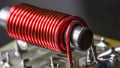
Featured Image used courtesy of Alpha and Omega Semiconductor