Facebook
 Google
 GitHub
 Linkedin
SiC - the High Performance Power Semiconductor
This article discusses the Silicon Carbide Technology with Chris Dries from USCi.
USCi (United Silicon Carbide, Inc.) is a major player in power electronics, specializing in the development of high-efficiency silicon carbide (SiC) devices with expertise in the Schottky barrier diodes, JFETs, MOSFETs, and solid-state circuit breakers. VIP interview with USCi-CEO and President Dr. J. Christopher Dries about his company and its positioning in the power electronics market.
Henning Wriedt: USCi was founded in 1998. What were the company charter and the founder's expertise at that time?
Christopher Dries: You’re correct Henning, USCi was founded quite some time ago. That original incarnation of the business began as many early-stage technology businesses begin . . . spinning out of a University. In the case of USCi, these origins began at Rutgers University, where the original founders had been working in SiC for some time, demonstrating at the research level the first of many types of SiC devices, Schottky Diodes, JFETs, MOSFETs, BJTs, and even early integrated circuits.
In my experience, however, it often takes much longer than original founders think to achieve commercial success. My own background is in InP and GaAs devices for optoelectronics. The scientific community knew that these devices were ideal for telecommunication systems as early as the 1970s and early 1980s, but did not achieve significant commercial success until the markets and materials matured in the 1990s and early 2000s.
Our current board and management team at USCi (who along with our employees own the company) recognized that SiC was in an early gestation period in 2009 when we purchased the assets of the business. Whether prescient or lucky, I believe that we have captured the market timing beautifully, matching USCi’s technology and manufacturing model with exponentially growing market demand.
Henning Wriedt: What makes Silicon Carbide so unique, compared to the current workhorse Silicon? Is it just the wide bandgap?
Christopher Dries: The fact that SiC is a wide bandgap material is certainly the basic physical reason it is unique, but the fact that it can be grown in bulk crystals as large as 150 mm is what makes it the leading commercial high-performance power semiconductor.
The bulk crystal structure enables SiC designers to build high cell density vertical current flow devices. This attribute coupled with USCi’s advanced thin wafer technology allows our team to compete with the most advanced Si transistors with more than 10X smaller die size. While SiC is still expensive, this advanced technology allows our team to provide cost-performance that exceeds anything that Si or even GaN can provide at present from 650 V and up.
Henning Wriedt: The first SiC devices were Schottky diodes, followed by junction-gate FETs and MOSFETs for high-power switching. What is next?
Christopher Dries: Basic switching functionality is really just the tip of the iceberg for SiC devices. At USCi, we believe that higher levels of functional integration are the future of our industry. While there will always be a home for discrete power switches, we can do much more through higher levels of integration, where we let each materials system do what it can do best.
For example, integrating our small die size SiC switch technologies with state of the art Si-based controllers and ICs is a simple way to provide enhanced value for our customers.
In addition, the utilization of half-bridge building blocks with integrated controllers is another higher level of value where we see the industry headed. Lastly, in USCi’s case, we see new topologies such as Totem-Pole PFC, enabled by our advanced switches overtaking traditional topologies such as boost PFC circuits.
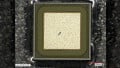
Figure 1: SiC manufacturing
Henning Wriedt: How is your current product portfolio structured?
Christopher Dries: I would argue that we have the broadest SiC technology portfolio in the world at present, spanning Schottky Diodes, JFETs for circuit protection, Cascodes for switching, MOSFETs for medium voltage, and Supercascodes for voltages > 3.3 kV. In addition, we manufacture these products on two geographically distinct manufacturing lines. One runs 100 mm wafers and the other runs 150 mm.
We have been careful not to get “in-love” with our own technology, but instead to be technology agnostic, using the best device for each voltage application. In the case of rectifiers, that is obviously JBS structure diodes. For switches from 650 V – 1700 V, Cascode devices, which incorporate a low-voltage MOSFET in series with a normally on JFET, are the ideal switch. For high Rds on applications (> 200 mohm) in the 1200 V range, one could make a good argument for a MOSFET due to the additional packaging cost of a Cascode.
For medium voltage applications, we see little differentiation between MOSFETs and Cascodes in overall performance, although the diode behavior here gives the edge to the Cascode. Lastly, at voltages > 3.3 kV, we believe nothing can beat the Supercasode in terms of ease of use, performance, and cost.
Henning Wriedt: Please explain your foundry services. Who are the typical customers for these services?
Christopher Dries: In our context, foundry services simply means that we are willing to run custom current or voltage rating devices for customers on any of our released platforms. For example, if a customer wants a 100 A 1700 V Schottky diode which is not in our standard portfolio, we are happy to run that device for them on our platform with the addition of a modest amount of NRE over and above our standard prices.
Henning Wriedt: How do you define custom devices for special applications?
Christopher Dries: Custom devices are different from our foundry services in the sense that they require some modification in addition to straightforward mask geometries to achieve the end customers’ goals. This may be using a special metallization to enable brazed lead manufacturing for a customer, or tailoring the device structure, doping, and overall characteristics to achieve a particular saturation characteristic in a JFET for a customer.
We have developed so much experience now in such a broad array of device types, that most modifications that a customer may want can be thoroughly developed and modeled in TCAD in such a way that we can hit a new device implementation on the first run.
Henning Wriedt: You concentrate on the development of normally OFF switch solutions. Is this driven by certain applications?
Christopher Dries: The world desires normally off devices for switching functions. This is why we developed our Cascode devices as the ideal SiC switch. They provide a universal gate drive, meaning they can use any standard Si drive solution whether it be an IGBT or high voltage MOSFET, while at the same time remain compatible with the unique -5 – 20 V drives of most SiC MOSFETs.
We provide this while providing a 4.5 V threshold, and body diode performance that rivals that of a SiC Schottky Diode. Our customers love them because they can simply drop them into any switch solution they are using and run at higher power density and higher efficiency, while not breaking the bank.
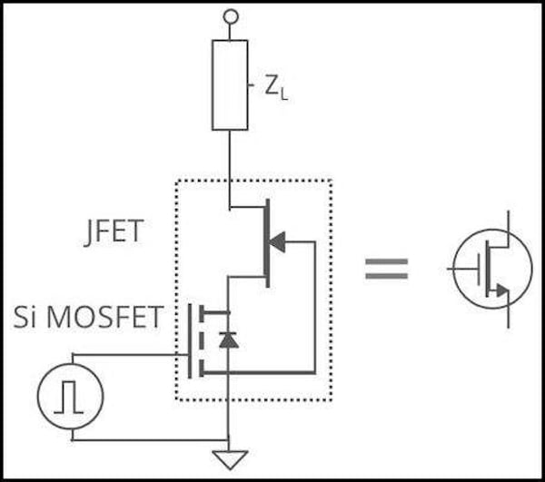
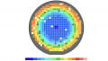
Figure 2: SiC Cascode configuration
Henning Wriedt: How significant is the Supercascode technology for your company?
Christopher Dries: The Supercascode is simply an extension of our standard Cascode technology to higher voltages, 3.3 kV and higher . . . the sky is the limit. The beauty of this technology is that it uses all of our standard off the shelf 1200 V or 1700 V FETs, an inexpensive voltage balancing network, and the entire switch is controlled by a single 30 V or so, high threshold voltage Si MOSFET. This means it is extremely easy to control with a standard gate drive, while having superior diode performance, while costing a fraction of the cost of any alternative wide-bandgap switch.
This technology is extremely important to our business as it will become a cornerstone of devices in traction and other high voltage applications such as solid-state transformers. As electrical distribution models change from using ohms law to distribute power through the path of least resistance, to systems that dynamically route power in through the most efficient route possible, we expect our supercascodes to be at the heart of these power routing systems.
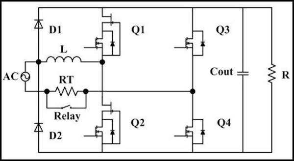
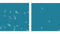
Figure 3: 1.5 kW Totem-pole PFC diagram
Henning Wriedt: What can the electronics industry expect from USCi in the upcoming two years?
Christopher Dries: With the success that we have achieved with our Cascode technologies in standard TO-247 and TO-220 package designs, you can expect a massive proliferation of our devices into source kelvin connected packages that enable our customers to extract the highest performance out of our devices.
We will also begin to deploy our Cascodes which incorporate a low voltage MOSFET and SiC JFET in stacked form. This means that the two devices will be provided as a single unit with the low voltage MOSFET bonded directly to the high voltage JFET producing a single die that performs as an ideal Si like high voltage switch.
Lastly, USCi will release our high-temperature capable IC platform within the next two years. This will enable our customers to design high temperature >300 °C circuits in our JFET platform for use in various hi-reliability applications.
Biography Dr. J. Christopher Dries, President and CEO
Chris Dries oversaw the acquisition of USCi in 2009 and has served as President and CEO ever since. In addition to his capacity as CEO, Chris serves as a member of the Board of Directors and is an Investor in the company.
Chris helped build and sell Sensors Unlimited to Finisar Corporation, participated in the buy-back of the business and then subsequent sale to Goodrich Corporation in 2005 where he served as VP of Research and Development of the Imaging business. Chris obtained his bachelor's degree from Duke University and Ph.D. from Princeton University, both in Electrical Engineering.
His various areas of expertise include photodetectors, OEICs, high-speed electronics and focal planes for hyperspectral imaging. He serves on the Princeton Graduate School Leadership Council, the Princeton Electrical Engineering Department Advisory Board and the Duke University Engineering School Board of Visitors. Dr. Dries earned a B.S. in Electrical Engineering from Duke University in 1994, an M.A. and a Ph.D. from Princeton University in 1996 and 1999, respectively. His thesis research was on the fabrication and use of strained layers of InGaAsP in photodetectors and quantum well lasers.
This article originally appeared in the Bodo’s Power Systems magazine.