Facebook
 Google
 GitHub
 Linkedin
Next-Gen Solar Cells Break Indoor Efficiency Records
Researchers have demonstrated a perovskite indoor solar cell with a record 37.6% power conversion efficiency under LED lighting.
University College London (UCL) researchers have reported a significant breakthrough in indoor photovoltaic technology, achieving a record 37.6% power conversion efficiency under LED lighting.
By refining the internal chemistry and structure of perovskite solar cells through a multi-layer “triple passivation” approach, the team has engineered devices that excel at harvesting ambient light and demonstrate long-term stability and scalability.

UCL researchers test the perovskite solar cells. Image used courtesy of UCL
More Efficiency With Triple Passivation
The key innovation is a multi-pronged passivation strategy that mitigates one of perovskite’s biggest problems: defect-induced recombination losses. The UCL team introduced three types of agents to address distinct issues at the grain boundaries, surfaces, and bulk of the perovskite layer.
Rubidium chloride served as a crystallization modulator, improving film uniformity and reducing voids. Meanwhile, dimethylammonium iodide (DMAI) and phenylethylammonium chloride (PEACl) each targeted different trap states, with DMAI addressing mobile ion migration and PEACl forming a 2D capping layer to enhance surface stability.
The result was a perovskite layer with exceptionally low trap density (4.86x1015cm-3) and long carrier diffusion lengths, contributing to higher efficiency and improved long-term reliability. Under indoor LED conditions, these triple-passivated devices maintained high open-circuit voltages and fill factors, outperforming untreated control cells by more than 6% absolute efficiency. The improvements remained consistent after 100 days of storage, with treated devices retaining 92% of their performance versus 76% in untreated samples.
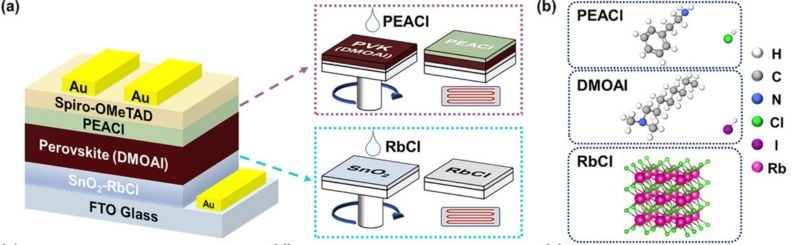
The wide-bandgap N-i-P PSC structure and the preparation process (a). Chemical structure of the three passivators (PEACl, DMOAI, and RbCl) (b). Image used courtesy of Huang et al.
Tuning the Bandgap for Artificial Light
Unlike traditional silicon photovoltaics, which are optimized for the solar spectrum, these perovskite devices were fine-tuned to maximize absorption under indoor lighting. The researchers selected a halide composition that produced a bandgap of 1.75 eV, ideal for harvesting visible light emitted by common LEDs and fluorescents. Combined with the material’s inherent high absorption coefficient and the optical clarity of the device stack, this made the architecture particularly well suited to ambient illumination.
To validate real-world performance, the team ran the cells under varied LED lighting conditions and extracted current-voltage curves, external quantum efficiency, and transient photovoltage decay. Notably, the devices operated near the theoretical efficiency limit for the given light source and maintained voltage output with minimal hysteresis, which is key to powering logic and sensing circuits without large energy storage buffers.
Toward Battery-Free Smart Devices
The implications of this work stretch well beyond laboratory benchmarks. With power conversion efficiencies exceeding 37% under ambient light, the UCL-developed perovskite cells are uniquely positioned to support next-generation indoor electronics, particularly IoT sensor networks, wearable health monitors, and low-power smart tags, without relying on batteries. Because these applications typically operate in low-light environments and demand only microwatts to milliwatts of power, pairing them with ultra-efficient indoor photovoltaics opens the door to maintenance-free and sustainable designs.
To explore this potential, the researchers demonstrated integration of their triple-passivated solar cells with logic-level loads under LED illumination. Even under reduced light intensity, the devices delivered enough voltage and current to directly power microcontrollers and sensor circuits, offering a practical proof-of-concept for battery-free electronics. Furthermore, the simplified planar architecture and compatibility with low-temperature solution processing suggest that these devices could be fabricated at scale and on flexible substrates.
The study appeared in Advanced Functional Materials.