Facebook
 Google
 GitHub
 Linkedin
Maximizing the Power Density of OBCs With GaN HEMT Devices
As sales of electric vehicles (EVs) grow, the performance requirements for onboard chargers (OBCs) are becoming increasingly demanding, with original equipment manufacturers looking to minimize the size and weight of these components to help improve vehicle range. In this article, we consider the design challenge, topology selection process, and features of maximizing the power density of OBCs with GaN HEMT devices.
As sales of electric vehicles (EVs) grow, the performance requirements for onboard chargers (OBCs) are becoming increasingly demanding, with original equipment manufacturers looking to minimize the size and weight of these components to help improve vehicle range.
Currently, the power density level that can be achieved in OBCs using silicon devices is typically 2 kW/L. Wide bandgap devices could make it possible to achieve power densities even beyond 6 kW/L, which would represent a 3 times improvement. Infineon used this figure as the target level of power density in the design of a three-phase 11 kw OBC using GaN HEMTs. In this article, we consider the design challenge, topology selection process, and features of the final design.
Onboard Charger Specifications
The main challenges when realizing a high-power density OBC are the wide input and output voltage range specifications. Grid voltages vary worldwide, adding complexity to the design of a PFC rectifier stage. The output voltage range depends on the EV battery voltages, representing a further challenge for the DC/DC stages. Balancing these requirements means choosing between hard-switching losses or increasing RMS currents, neither of which is desirable. In addition, as more renewable forms of electricity begin to supply the grid, the peak power trimming provided by connected EVs is considered a means by which the grid can be stabilized, further complicating the design task because the OBC now also requires bidirectional power processing.
A final design specification is that OBCs must be able to operate from single- and three-phase grid supplies. Assuming the available current in each phase is limited by a fuse, a 230 Vrms (line-to-neutral) phase with a 16 A-rated fuse can provide 3.6 kW of single-phase power and 11 kW of three-phase power. While this is possible for a traditional three-phase system (e.g., a Vienna rectifier), for the same OBC to operate in the United States, a 240 Vrms split single-phase grid interface with a 40 A fuse would be required for 9.6 kW of power.
Selecting an OBC Topology
An existing 10 kW EV charger with a power density of 10 kW/L was used as a starting point in the quest to maximize the power density of the OBC design. The specifications for this charger are shown in Table 1.

Table 1. Design specifications for 10 kW EV charger
The final charger design (Figure 1) used a Vienna rectifier PFC with a regulated split DC-link, to which four cascaded Dual Active Bridges (DABs) DC/DC converters with 600 V rated GaN HEMTs (IGOT60R042D1) were connected to provide output voltage regulation. By their very nature, DABs are bidirectional topologies that can perform ZVS in buck and boost modes, making them suitable for high-frequency operation in EV chargers and OBCs. By replacing the rectifier diodes of the Vienna rectifier PFC with active switches, synchronous rectification, and fully bidirectional power conversion are possible.

Figure 1. Topology combining Vienna rectifier with DABs
OBC Design Features
The higher power density was made possible by three key features of this design. First, a novel 1/3-PWM synergetic modulation scheme operating at 560 kHz uses the DC-DC stage to control the DC-link voltage, so in the AC/DC stage, only one of the three phases is switching at any time. This has the advantage of reducing power dissipation caused by the switching losses in the AC/DC stage and also allows the DC-link voltage to be reduced to the lowest possible for a boost topology, i.e., to the six-pulse envelope of the line-to-line voltages and/or the maximum line-to-line voltage. This also has an advantage for the DC/DC stage by reducing the voltage transfer ratio required in subsequent DC/DC converters. For example, with a minimum system output voltage of 250 V, the DC-link voltage does not require boosting to the maximum line-to-line voltage - a six-pulse shape between 490-565 V, thereby lowering the voltage range of the buck converter.
Second, the DABs are modulated using the degrees of freedom of the duty cycles, phase shift, and switching frequency to achieve ZVS over a wide input and output voltage range. A topology with two active full bridges allows voltage to be controlled over a wide range. However, there is a challenge in determining the optimal balance between the switching losses and the conduction losses in the transformer and semiconductor devices. The most favorable operating point for the DABs is the one where the voltage transfer ratio between the primary and the secondary is the same as the turns ratio, where low RMS currents are present, as well as ZVS transitions in all the bridge legs. However, when modulating the DAB beyond the natural voltage transfer ratio, advanced modulation schemes can be used to minimize the losses for a given set of operating parameters. Under these conditions, the degree of freedom is the phase shift between the primary and the secondary side, allowing the power flow from primary to secondary (or vice versa) to be controlled.
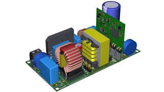
Finally, compared to silicon and silicon carbide devices, GaN GIT HEMT devices have smaller output capacitance for the same on-resistance, thereby enabling full ZVS at lower current levels. They also have exceptionally low specific Rdson values and have the ability to operate in both partial-hard and hard-switched modes. By combining advanced control and modulation schemes with the superior behavior of GaN devices under different switching conditions, the desired level of power density required for next-generation OBCs for EVs could be achieved. The uncased power density of the final EV charger design (Figure 2), which measured 17.8 x 400 x 140 mm, was 10kW/L.

Figure 2. PCB of GaN-based EV charger solution
Takeaways of GaN HEMTs
GaN HEMTs have inherent features making them suitable for high-frequency operations, which enable them to operate in both hard- and soft-switching regimes. This allows them to be used in advanced modulation and control schemes, making it possible to achieve wide input and output voltage ranges in designs with high power density. Infineon has demonstrated that these devices will make it possible to realize the level of power density required for next-generation OBC chargers in EVs. To learn more about Infineon’s HEMT GaN solutions, click here.