Facebook
 Google
 GitHub
 Linkedin
8 Steps to Designing an LLC Resonant Converter
This article provides a step-by-step guide for designing an LLC resonant converter with a half-bridge configuration on the primary side and a center-tapped transformer on the secondary side to optimize performance.
LLC resonant converters have become a cornerstone in power electronics. They are widely adopted across various markets because they can achieve high efficiency while minimizing electromagnetic interference (EMI) through soft-switching techniques. LLC topology offers several configurations optimized for specific applications. In particular, there are two prominent configurations for the primary side and two different methods for the secondary side.
![]()
Image used courtesy of Adobe Stock
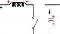
Half-Bridge LLC Resonant Converter Design With a Center-Tapped Transformer
This section explores the detailed design process for a half-bridge LLC resonant converter using a center-tapped transformer (see Figure 1). Efficient power conversion can be achieved by combining the advantages of LLC topology with the flexibility of a center-tapped transformer.
![]()
Figure 1. Half-Bridge LLC Resonant Converter with a Center-Tapped Transformer. Image used courtesy of MPS
Figure 2 shows a flowchart of the meticulous step-by-step approach for designing an LLC resonant converter, which is described in further detail in the following sections.
![]()
![]()
![]()
![]()
Figure 2. Step-by-Step Flowchart for LLC Resonant Converter Design. Image used courtesy of MPS
Design Consideration
Two key design considerations can significantly impact the efficiency and performance of the LLC resonant converter:
Optimizing the resonant inductance ratio (LN): A higher LN typically improves efficiency under heavy-load conditions. It is recommended to maintain LN within the 4 to 10 range to balance efficiency and component stress.
Selecting an appropriate quality factor (QE): To prevent excessive voltage stress on the resonant capacitor and minimize high inrush currents during start-up, QE must be maintained within the 0.34 to 0.49 range. This range ensures a good tradeoff between minimizing stress and maintaining overall converter performance.
Step 1: Determine the Converter Specifications
Table 1 shows the specifications of an example LLC resonant converter.
Table 1. Specifications of Example LLC Resonant Converter
|
Parameters |
Values |
Units |
|
Input voltage (VIN) |
400 |
VDC |
|
Output voltage (VOUT) |
48 |
VDC |
|
Output power (POUT) |
600 |
W |
|
Resonant frequency (fR) |
100 |
kHz |
|
Minimum switching frequency (fSW_MIN) |
50 |
kHz |
|
MOSFET output capacitance |
80 |
pF |
Step 2: Transformer Turns Ratio
When calculating the transformer turns ratio (n), the gain (G) must be equal to 1 to work at the resonant frequency (fR). n can be calculated with Equation (1):
\[n=\frac{N1}{N2}=\frac{V_{IN}}{2\times V_{OUT}}\times G\Rightarrow n=\frac{400}{2\times48}\times1\Rightarrow n=4.17\,\,\,\,\,(1)\]
Where n = 4.17 can be rounded to a whole number so nLLC = 4.
Step 3: Determine the Maximum Magnetizing Inductance
To calculate the maximum magnetizing inductance (LM_MAX), the following parameters must be determined: maximum dead time (tDEAD_MAX), minimum switching period (tSW_MIN), and output capacitance of the primary-side MOSFET (COSS).
The HR1002A, an enhanced LLC controller, is selected for this design due to its proven reliability under varying operational conditions. Based on the HR1002A datasheet, the controller’s tDEAD_MAX is 2µs. The output capacitance of the selected MOSFET (COSS) is 80pF.
tSW_MIN can be calculated with Equation (2):
\[t_{SW\_MIN}=\frac{1}{f_{START\_UP}}\Rightarrow\\\Rightarrow t_{SW\_MIN}=\frac{1}{3\times f_{SW}}\Rightarrow\\\Rightarrow t_{SW\_MIN}=\frac{1}{3\times100kHz}\Rightarrow\\\Rightarrow t_{SW\_MIN}=3.33\mu s\,\,\,\,\,(2)\]
LM_MAX can be calculated with Equation (3):
\[L_{M\_MAX}=t_{MIN}\times\frac{t_{DEAD\_MAX}}{16\times C_{OSS}}\Rightarrow L_{M\_MAX}=3.3\mu s\times\frac{2\mu s}{16\times 80pF}\Rightarrow L_{M\_MAX}=5.2mH\,\,\,\,\,(3)\]
Step 4: LN and QE Selection
As discussed regarding design considerations, QE is recommended to be within the range shown in Equation (4):
\(\frac{1}{3}\text{<}Q_{E}\text{<}\frac{1}{2}\Rightarrow\,0.33\text{<}Q_{E}\text{<}0.5\,\,\,\,\,(4)\)
In addition, QE is related to the resonant capacitor voltage stress and inrush current during start-up. Therefore, QE is selected to be 0.35, which is near the minimum.
Similar to QE, the LN ratio is recommended to be within the range shown in Equation (5):
\[4\leq L_{N}\leq 10\,\,\,\,\,(5)\]
To stabilize efficiency across all the load ranges, it is recommended to use an LN ratio between 4 and 6. To prioritize efficiency at the maximum output power (POUT), it is recommended to use an LN ratio between 6 and 10. In the example LLC resonant converter, LN is selected to be 9.
Step 5: Resonant Tank Selection
To select the resonant tank, the following parameters must be determined: load resistance (RL), equivalent load resistance (RE), resonant capacitor (CR), resonant inductor (LR), and magnetizing inductance (LM).
RL can be calculated with Equation (6):
\[R_{L}=\frac{V^{\,\,\,\,\,\,\,\,\,\,\,2}_{OUT}}{P_{OUT}}\Rightarrow R_{L}=\frac{48^{2}}{600}\Rightarrow R_{L}=3.84\Omega\,\,\,\,\,(6)\]
RE can then be calculated with Equation (7):
\[R_{E}=\frac{8\times n_{LLC}^{\,\,\,\,\,\,\,\,\,\,\,2}}{\pi^{2}}\times R_{L}\Rightarrow R_{E}=\frac{8\times4^{2}}{\pi^{2}}\times3.84\Rightarrow R_{E}=49.8\Omega\,\,\,\,\,(7)\]
CR can be calculated with Equation (8):
\[C_{R}=\frac{1}{2\times\pi\times f_{R}\times R_{E}\times Q_{E}}\Rightarrow C_{R}=\frac{1}{2\times\pi\times100kHz\times49.8\times0.35}\Rightarrow C_{R}=91.31nF\,\,\,\,\,(8)\]
It is recommended that CR be rounded to the nearest standard capacitance or that capacitors be placed in parallel to obtain the closest value. In this case, two 47nF capacitors are used in parallel for a total capacitance of 94nF.
LR can be calculated with Equation (9):
\[L_{R}=\frac{1}{(2\times\pi\times f_{R})^{2}\times C_{R}}\Rightarrow L_{R}=\frac{1}{(2\times\pi\times100kHz)^{2}\times94nF}\Rightarrow L_{R}=26.95\mu H\,\,\,\,\,(9)\]
Where LR = 26.95µH can be rounded to 27µH.
LN can be calculated with Equation (10):
\[L_{N}=\frac{L_{M}}{L_{R}}\Rightarrow L_{M}=L_{N}\times L_{R}\Rightarrow L_{M}=9\times27\mu H\Rightarrow L_{M}=243\mu H\,\,\,\,\,(10)\]
LM can be checked with Equation (11):
\[L_{M}\leq L_{M\_MAX}\Rightarrow243\mu H\leq5.2mH\,\,\,\,\,(11)\]
Step 6: Recalculation with the Final Values of LR, CR, and LM
The resonant frequency (fR) can be recalculated with the final values of LR, CR, and LM using Equation (12):
\[L_{R}=\frac{1}{(2\times\pi\times f_{R})^{2}\times C_{R}}\Rightarrow\\\Rightarrow 2\times\pi\times f_{R}=\frac{1}{\sqrt{L_{R}\times C_{R}}}\Rightarrow\\\Rightarrow f_{R}=\frac{1}{2\times\pi\times\sqrt{L_{R}\times C_{R}}}\Rightarrow\\\Rightarrow f_{R}=\frac{1}{2\times\pi\times\sqrt{27\mu H\times94nF}}\Rightarrow\\\Rightarrow f_{R}=99.9kHz\,\,\,\,\,(12)\]
QE can be recalculated with the final values of LR, CR, and LM using Equation (13):
\[C_{R}=\frac{1}{2\times\pi\times f_{R}\times R_{E}\times Q_{E}}\Rightarrow\\\Rightarrow Q_{E}=\frac{1}{2\times\pi\times f_{R}\times R_{E}\times C_{R}}\Rightarrow\\\Rightarrow Q_{E}=\frac{1}{2\times\pi\times99.9kHz\times49.8\times94nF}\Rightarrow\\\Rightarrow Q_{E}=0.34\,\,\,\,\,(13)\]
Where QE must be within the recommended range: 0.33 < QE < 0.5 0.33 < 0.34 < 0.5.
If QE is outside the specified range, adjust CR and then repeat the calculations for Equation (8) through Equation (13).
Step 7: Checking the Results
To check the results, fN, G, and VIN are used to obtain the tank resonant voltage transfer function. Then, VOUT is validated to ensure the converter’s proper operation. The resonant tank and gain can be verified using plots.
Tank Resonant Voltage Transfer Function
To ensure that the converter works in fR, the following is assumed:
\[f_{N}=\frac{f_{SW}}{f_{R}}=1\Rightarrow f_{SW}=f_{R}=99.9kHz\]
The parameters are then replaced in the tank resonant voltage transfer function, G(fN), which can be calculated with Equation (14):
\[G(fN)=\frac{1}{\sqrt{\Big[1+\frac{1}{L_{N}}-\frac{1}{f_{N}^{\,2}\times L_{N}}\Big]^{2}+Q_{E}^{\,\,\,\,2}\times\Big(\frac{1}{f_{N}}-f_{N}\Big)^{2}}}\Rightarrow\\\Rightarrow G(1)=\frac{1}{\sqrt{\Big[1+\frac{1}{9}-\frac{1}{1^{2}\times 9}\Big]^{2}+0.34^{2}\times\Big(\frac{1}{1}-1\Big)^{2}}}\Rightarrow\\\Rightarrow G(1)=1\,\,\,\,\,(14)\]
Output Voltage
The output voltage (VOUT) can be calculated with Equation (15):
\[V_{OUT}=\frac{V_{IN}}{2\times n_{LLC}}\times G\Rightarrow V_{OUT}=\frac{400}{2\times4}\times1\Rightarrow V_{OUT}=50V\,\,\,\,\,(15)\]
With a unity gain, VOUT is 50V instead of 48V.
There are two different methods to adjust VOUT. The first method is to reduce the gain below 1, which can be calculated with Equation (16):
\[V_{OUT}=\frac{V_{IN}}{2\times n_{LLC}}\times G\Rightarrow G=\frac{V_{OUT}\times2\times n_{LLC}}{V_{IN}}\Rightarrow G=\frac{48\times2\times4}{400}\Rightarrow G=0.96\,\,\,\,\,(16)\]
The converter works at the normalized switching frequency (fN), which has a ratio of about 1.2. fN can be found solving equation (14) or plotting the resonant tank at the 0.96 gain (see Figure 4).
fSW can be calculated with Equation (17):
\[f_{N}=\frac{f_{SW}}{f_{R}}\Rightarrow f_{SW}=f_{N}\times f_{R}\Rightarrow f_{SW}=1.2\times99.9kHz\Rightarrow f_{SW}=119.88kHz\,\,\,\,\,(17)\]
It is common to work within the fR range instead of at the exact fR due to components’ tolerances.
The second method to adjust VOUT is by modifying the input voltage (VIN), which can be calculated with Equation (18):
\[V_{OUT}=\frac{V_{IN}}{2\times n_{LLC}}\times G(f_{N})\Rightarrow\\\Rightarrow V_{IN}=\frac{V_{OUT}\times2\times n_{LLC}}{G(f_{N})}\Rightarrow\\\Rightarrow V_{IN}=\frac{48\times2\times4}{1}\Rightarrow\\\Rightarrow V_{IN}=384V\,\,\,\,\,(18)\]
By adjusting VIN to 384V, the converter operates at fR.
Verifying the Resonant Tank and Gain with Plots
The most effective way to validate the calculations is by plotting the tank resonant voltage transfer function using Equation (14) as well as plotting the gain using Equation (16). Consider the following two scenarios for the resonant tank gain.
In the first scenario, VIN = 400V, LR = 27µH, CR = 94nF, and LM = 243µH. Figure 3 shows the resonant tank gain at VIN = 400V with 0.96 gain.
![]()
Figure 3. Resonant Tank Gain at VIN = 400V, Gain = 0.96, and fN = 1. Image used courtesy of MPS
At fR, the gain is higher than necessary. To lower the gain to 0.96, the normalized frequency (fN) must be determined.
Figure 4 shows the resonant tank gain after adding the calculated gain. The 1.2 ratio of fN coincides with the 0.96 gain, which is indicated by the grey and black dashed lines.
![]()
Figure 4. Resonant Tank Gain at VIN = 400V, Gain = 0.96, and fN = 1.2. Image used courtesy of MPS
In the second scenario, VIN is reduced to 384V, while the other conditions remain the same (LR= 27µH, CR = 94nF, and LM = 243µH). Figure 5 shows the resonant tank gain at VIN = 384V, where the converter operates at fR with a unity gain.
![]()
Figure 5. Resonant Tank Gain at VIN = 384V. Image used courtesy of MPS
The second scenario is applied for step 8 and the final design, which are described below.
Step 8: Calculating the Current and Voltage Stress of the LLC Converter
The current and voltage stress of the LLC converter includes the tank resonant stress, the primary-side semiconductor devices’ stress, and the secondary-side semiconductor devices’ stress.
Tank Resonant Stress
The tank resonant stress is determined by the magnetizing peak inductance current (ILM_PEAK), resonant inductor RMS current (ILR_RMS), resonant peak inductor current (ILR_PEAK), and resonant capacitor voltage (VCR).
ILM_PEAK can be estimated with Equation (19):
\[I_{LM\_{PEAK}}=\frac{n_{LLC}\times V_{OUT}}{4\times L_{M}\times f_{R}}\Rightarrow I_{LM\_PEAK}=\frac{4\times48}{4\times243\mu H\times99.9kHz}\Rightarrow I_{LM\_PEAK}=1.98A\,\,\,\,\,(19)\]
ILR_RMS can be calculated with Equation (20):
\[I_{LR\_RMS}=\frac{V_{OUT}\times\sqrt{4\times\pi^{2}+n_{LLC}^{\,\,\,\,\,\,\,\,\,\,\,4}\times R_{L}^{\,\,\,2}\times\Big(\frac{1}{L_{M}\times f_{R}}\Big)^{2}}}{4\times\sqrt{2}\times n_{LLC}\times R_{L}}\Rightarrow\\\Rightarrow I_{LR\_RMS}=\frac{48\times\sqrt{4\times\pi^{2}+4^{4}\times 3.84^{2}\times\Big(\frac{1}{243\mu H\times 99.9kHz}\Big)^{2}}}{4\times\sqrt{2}\times 4\times 3.84}\Rightarrow I_{LR\_RMS}=3.74A\,\,\,\,\,(20)\]
ILR_PEAK can be calculated with Equation (21):
\[I_{LR\_PEAK}=\sqrt{2}\times I_{LR\_{RMS}}\Rightarrow I_{LR\_{PEAK}}=\sqrt{2}\times3.74\Rightarrow I_{LR\_PEAK}=5.29A\,\,\,\,\,(21)\]
VCR can be calculated with Equation (22):
\[V_{CR}=\frac{I_{LR\_RMS}}{2\times\pi\times f_{R}\times C_{R}}\Rightarrow V_{CR}=\frac{3.74}{2\times\pi\times99.9kHz\times94nF}\Rightarrow V_{CR}=63.39V\,\,\,\,\,(22)\]
Stress of Primary-Side Semiconductor Devices
The stress of primary-side semiconductor devices is determined by the voltage stress of the primary side (VQ1), peak current of the primary side (IQ1_PEAK), and the RMS current of the primary side (IQ1_RMS).
VQ1 can be calculated with Equation (23):
\[V_{Q1}=V_{Q2}=V_{IN}=384V\,\,\,\,\,(23)\]
IQ1_PEAK can be calculated with Equation (24):
\[I_{Q1\_PEAK}=I_{Q2\_PEAK}=I_{LR\_PEAK}=5.29A\,\,\,\,\,(24)\]
IQ1_RMS can be calculated with Equation (25):
\[I_{Q1\_{RMS}}=I_{Q2\_{RMS}}=\frac{V_{OUT}\times\sqrt{4\times\pi^{2}+n_{LLC}^{\,\,\,\,\,\,\,\,\,\,4}\times R_{L}^{\,\,\,2}\times\Big(\frac{1}{L_{M}\times f_{R}}\Big)^{2}}}{8\times n_{LLC}\times R_{L}}\Rightarrow\\\Rightarrow I_{Q1\_{RMS}}=I_{Q2\_{RMS}}=\frac{48\times\sqrt{4\times\pi^{2}+4^{4}\times 3.84^{2}\times\Big(\frac{1}{243\mu H\times 99.9kHz}\Big)^{2}}}{8\times 4\times 3.84}\Rightarrow\\\Rightarrow I_{Q1\_RMS} = I_{Q2\_RMS} = 2.65A\,\,\,\,\,(25)\]
A high LN means LM is high as well, which reduces the RMS current in semiconductor devices.
Stress of Secondary-Side Semiconductor Devices
The stress of secondary-side semiconductor devices is determined by the voltage stress of the secondary side (VQ3), peak current of the secondary side (IQ3_PEAK), and the RMS current of the secondary side (IQ3_RMS).
VQ3 can be calculated with Equation (26):
\[V_{Q3}=V_{Q4}=2\times V_{OUT}\Rightarrow V_{Q3}=V_{Q4}=2\times48\Rightarrow V_{Q3}=V_{Q4}=96V\,\,\,\,\,(26)\]
IQ3_PEAK can be calculated with Equation (27):
\[I_{Q3\_PEAK}=I_{Q4\_PEAK}=\sqrt{12}\times\frac{V_{OUT}\times\sqrt{12\times\pi^{4}+\frac{5\times\pi^{2}-48}{L_{M}^{\,\,\,\,2}\times f_{R}^{\,\,\,2}}\times n_{LLC}^{\,\,\,\,\,\,\,\,\,\,\,4}\times R_{L}^{\,\,\,2}}}{24\times\pi\times R_{L}}\Rightarrow\\\Rightarrow I_{Q3\_PEAK}=I_{Q4\_PEAK}=\sqrt{12}\times\frac{48\times\sqrt{12\times\pi^{4}+\frac{5\times\pi^{2}-48}{(243\mu H)^{2}\times (99.9kHz)^{2}}\times 4^{4}\times 3.84^{2}}}{24\times\pi\times 3.84}\Rightarrow\\\Rightarrow I_{Q3\_PEAK}=I_{Q4\_PEAK}=19.71A\,\,\,\,\,(27)\]
IQ3_RMS can be calculated with Equation (28):
\[I_{Q3\_RMS}=I_{Q4\_RMS}=\sqrt{3}\times\frac{V_{OUT}\times\sqrt{12\times\pi^{4}+\frac{5\times\pi^{2}-48}{L_{M}^{\,\,\,\,2}\times f_{R}^{\,\,\,2}}\times n_{LLC}^{\,\,\,\,\,\,\,\,\,\,\,4}\times R_{L}^{\,\,\,2}}}{24\times\pi\times R_{L}}\Rightarrow\\\Rightarrow I_{Q3\_RMS}=I_{Q4\_RMS}=\sqrt{3}\times\frac{48\times\sqrt{12\times\pi^{4}+\frac{5\times\pi^{2}-48}{(243\mu H)^{2}\times (99.9kHz)^{2}}\times 4^{4}\times 3.84^{2}}}{24\times\pi\times 38.4}\Rightarrow\\\Rightarrow I_{Q3\_RMS}=I_{Q4\_RMS}=9.85A\,\,\,\,\,(28)\]
Final Design
By calculating the current and voltage stresses on the resonant tank and semiconductor devices, the LLC converter design using the HR1002A can be completed. Table 2 shows the design results.
Table 2. Design Results
|
Parameters |
Values |
Units |
|
Input voltage |
384 |
V |
|
Magnetizing inductance |
243 |
µH |
|
Transformer turns ratio |
4 |
- |
|
Resonant inductance |
27 |
µH |
|
Resonant capacitance |
94 |
nF |
|
Peak current (Q1, Q2, and LR) |
5.29 |
A |
|
RMS current: Q1, Q2, and LR) |
2.65 |
A |
|
Resonant capacitor voltage |
63.39 |
V |
|
Peak current (Q3 and Q4) |
19.71 |
A |
|
RMS current (Q3 and Q4) |
9.85 |
A |
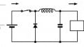
The HR1002A is an enhanced LLC controller that provides robust adaptative dead-time adjustment (ADTA) as well as several protections, including shoot-through and capacitive mode protection (CMP) to avoid hard switching. There are also two over-current protection (OCP) levels, where one level provides a configurable delay for enhanced surge performance. Brown-in and brownout thresholds set the minimum VIN at which the converter can start working.
Due to the capabilities of the HR1002A, the power converter stage also requires only a few external components to function effectively.
Figure 6 shows the schematic of the half-bridge LLC with a center-tapped transformer using the HR1002A.
![]()
Figure 6. Half-Bridge LLC with a Center-Tapped Transformer Using the HR1002A. Image used courtesy of MPS
LLC Topology in Real-World Applications
Selecting the LLC topology for the primary and secondary sides is critical for optimizing performance across various applications. The half-bridge LLC with a center-tapped transformer is ideal for power levels up to 1 kW.
By adhering to the design principles discussed in this article, including optimizing the resonant inductance ratio and quality factor, engineers can ensure that converters operate within the desired parameters while reducing the risk of component failure. Moreover, the HR1002A controller further enhances LLC converter designs with its advanced protection features, ensuring reliability and durability in real-world applications.
For more solution options, explore MPS's selection of integrated, high-reliability LLC controllers.