Facebook
 Google
 GitHub
 Linkedin
SMT Hybrid Packaging 2015 How to Package Future Power Components
This article discusses the Surface Mount Technology Hybrid Packaging 2015, an exhibition aimed to inform visitors about the latest trends in semiconductor.
SMT Hybrid Packaging is the exhibition which informs its visitors about newest trends in semiconductor, PCB and systems manufacturing technologies. This year´s main topic was packaging technologies for smart systems at wafer and panel level which creates impact
on power components, too.
New at SMT Hybrid Packaging 2015 was the “High Tech PCB Area” in which companies presented their products and services regarding the PCB topic. The integrated forum and the catering area enabled discussions about developments and trends. “Man – Machine – Collaboration - Technology produces emotions, emotions control Technolgy” was the topic of the production line 2015. Initiated by Fraunhofer IZM Berlin, exhibitors at the “Optics meets Electronics” joint stand were showed the effects of the introduction of optical technologies in electronics and available solutions. At the joint stand of the 3-D MID network, 16 companies and institutes from all areas of interdisciplinary MID technology informed about the current status of technology and new serial applications. The formal presentation of the MID Industry Award 2015 took place on the MID forum.

Klaus-Dieter Lang, chairman of the SMT Hybrid Packaging committee defined in his presentation „Packaging Technologies for Smart Systems at Wafer and Panel Level“, customer requirements for smart systems. Smart systems are one of the actual mega-trend
in the electronics industry because there is no doubt that our world becomes smarter and smarter. Examples are Smart Cities, Smart Homes, Smart Healthcare, Smart Cars, Smart Watches, and even Smart Clothes and all of them need power supplies. Therefore these smart systems have to be connected, operate autonomously and safe, and be miniaturized. This creates impact on system integration and assembly. The robust, modular, and standardized systems must be produced at very low cost and energy-efficient with improved materials and advanced technologies for different application environments. They must transmit high volumes of data or pre-assessment of data with large bandwidth in real time over long ranges via high performance wired or wireless technologies. They require also the analysis of very large amounts of data, so called Big Data, as well as an extremely high level of data security which includes high reliability of data identification and no chance for manipulation. These systems should also include navigation capability and an intuitive human-machine interface for ease of use.
These customer requirements lead to the following driving forces for system packaging. There is increased functional integration in the minimized systems what means passive components are integrated in RDL and systems-in-package (SiP) as well as 3D capabilities are used to create the smallest possible dimensions. Future systems have to have the thinnest packages with minimum lateral area. But theses systems need to have also the maximum electrical performance e.g. minimum interconnect line length and reduced number of interconnects, multilayer RDL, and increased operating speeds. Hence the power consumption of theses dense packages is increasing what results in challenges for the thermal performance of the small chips with a high number of I/O and small pitches. Therefore the system requires improved chip to board coupling to overcome the thermal issues. And last but not least the entire production costs (batch processing, packaging, test) of the systems must be at minimum.
The solution for all of these challenges is wafer level packaging. Beside the increasing density of the chip packages via 3D technologies there is also the trend to embed PCB technologies to create a so called PLP (panel level package). This requires advanced PCB processes and materials ready for PLP as well as improved resolution and accuracy for next generation PLP. 2015 is - according to Yole Development - the starting point for the general use of real 3D chips with TSV (through silicon via) and 3D FOWLP (fan-out wafer level package). In its new report “Fan-Out and Embedded Die: Technologies and Market” Yole analysts mentioned that the FOWLP market reaches almost 200 Million Dollar and is expected to grow with 30% GAGR. After describing in detail the various methods of wafer level integration, silicon-interposer roadmap, the embedding process for PLP, panel level molding including PCB embedding substrates, IC substrate technologies, and the market for 3D components, Lang concludes that the production of embedded packages is ramping up fast. The market volume in 2013 was according to Yole 340 million dollars and is forecasted to reach 1700 million dollar in 2016. Driving forces for this growth are smart phones and computers. In smart phones DC/DC converters, power management units, and connectivity modules will be produced with embedded package technology in future.
MOSFET packages and driver MOS SiPs are the main applications in the computer market. PCB embedding technology is already implemented at PCB manufacturers, semiconductor manufacturers, and OSATs (outsourced semiconductor and test) or will come soon. To embed active components like integrated power management devices in laminate packages, power devices like voltage regulators, automotive modules including embedded IGBTs, RF modules, FOWLP, and PoP (package on package) with embedded application processor opens great market opportunities. The market volume for these embedded power modules was - according to TechSearch International - 727.5 Million Dollar in 2012 and will grow to 2,444.8 million dollar in 2017.
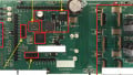
How to produce smart systems with these future devices was demonstrated at the joint booth Future Packaging by 36 electronic production companies. The sample board featured Flip-Chip components, SiP-om Board, 008004 components, SMD crimp connectors, tiny micro push button, Al bonds, and flex-rigid printed board to create a folded cube. This board was manufactured several times during the exhibition with commentary in English.