Facebook
 Google
 GitHub
 Linkedin
How to Create Bandpass Filters
This article explores the high-pass, low-pass combination technique used to create bandpass filters, as well as series resonant and parallel resonant bandpass filters, which provide different approaches to achieving a frequency response.
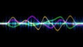
A bandpass filter is an electronic circuit that allows a specific range of frequencies to pass through while attenuating frequencies outside that range. It is commonly used in audio and radio frequency applications to selectively filter out unwanted frequencies and isolate the desired signal.
Image used courtesy of Adobe Stock
Understanding the operating principle of bandpass filters is important in designing and implementing circuits for signal processing and communication systems.
Constructing a Bandpass Filter
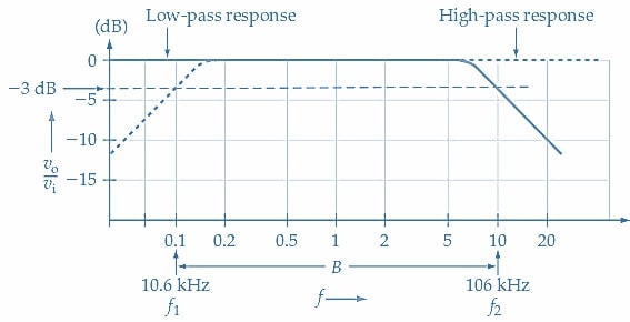
Figure 1(a) shows how a bandpass filter can be constructed by simply cascading high-pass and low-pass stages. The typical gain/frequency response for this arrangement is shown in Figure 1(b). The cutoff frequency of the high-pass circuit \(\Big(f_{c(H)}\Big)\) becomes the low cutoff frequency (f1) for the bandpass filter, and the cutoff frequency for the low-pass circuit \(\Big(f_{c(L)}\Big)\) becomes the high cutoff frequency (f2), as illustrated. For example, if \(\Big(f_{c(H)}\Big)\) is 10 kHz and \(f_{c(L)\) is 100 kHz, the high-pass circuit blocks signal frequencies below 10 kHz, and the low-pass filter blocks frequencies above 100 kHz. Consequently, only signals with frequencies between 10 kHz and 100 kHz will pass through both filters. A bandpass filter constructed this way should have at least a decade difference between f1 and f2. With a smaller difference, the second stage tends to load the first stage and thus affects its cutoff frequency. So, cascading of high-pass and low-pass filters is suitable only for constructing wide-band bandpass filters.
As shown in Figure 1(b), the bandwidth (B) of the circuit is
\[B=f_{2}-f_{1}\,(1)\]
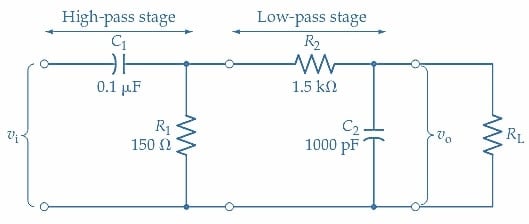
(a) Bandpass filter constructed of high-pass and low-pass stages.
(b) Bandpass frequency response of combined stages.
Figure 1. Bandpass filter consisting of cascaded high-pass and low-pass stages. The high-pass stage blocks signal frequencies up to f1, and the low-pass stage blocks frequencies above f2, thus passing the band of frequencies between f1 and f1. Image used courtesy of Amna Ahmad
The Centre frequency (fo) for a bandpass filter is defined as the geometric mean,
\[f_{o}=\sqrt{f_{1}\times f_{2}}\,(2)\]
Example 1
Determine the cutoff frequencies for the bandpass filter shown in Figure 1(a). Also, calculate the passband Centre frequency (fo).
Solution
High-pass stage
\[f_{cH}=\frac{1}{2\pi R_{1}C_{1}}=\frac{1}{2\pi\times150\Omega\times0.01\mu F}=10.6kHz \]
Low-pass stage
\[f_{cL}=\frac{1}{2\pi R_{1}C_{1}}=\frac{1}{2\pi\times1.5\Omega\times1000p F}=106kHz\]
Center frequency
\[f_{o}=\sqrt{f_{1}\times f_{2}}=\sqrt{f_{cH}\times f_{cL}}\]
\[=\sqrt{10.6kHz\times106kHz}=33.5kHz\]
Series Resonant Bandpass Filters
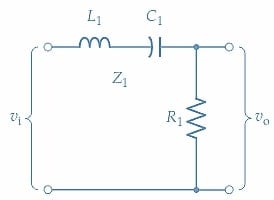
A bandpass filter using a series resonant circuit is shown in Figure 2(a), and its typical gain/frequency response is illustrated in Figure 3. The total impedance of the series RLC circuit is
\[Z=\Big(R_{1}+R_{W}\Big)+j\Big(X_{L}-X_{C}\Big)\]
Where RW is the resistance of the inductor winding. As shown by the filter equivalent circuit in Figure 2(b), the input voltage vi is divided across the impedance of the resonant circuit (Z1) and the resistor (R1) to produce the output voltage vo.
The voltage gain (attenuation) is
\[\frac{v_{_o}}{v_{_i}}=\frac{R_{1}}{R_{1}+Z_{1}}\,(3)\]
(a) Series-resonant bandpass filter circuit.
(b) R1 and Z1 are voltage dividers.
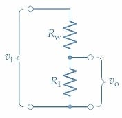
(c) At resonance Z1=RW.
Figure 2. In a series-resonant bandpass filter, input voltages are divided across the series LC circuit impedance (Z1) and the resistor (R1). When Z1 is a minimum at the resonance frequency, input voltages are passed to the output with little attenuation. Because Z1 becomes quite large at frequencies above and below resonance, inputs with off-resonance frequencies are severely attenuated. Image used courtesy of Amna Ahmad
The impedance of the LC circuit is a minimum at resonance and, consequently, \(\frac{v_{_o}}{v_{_i}}\) is a maximum. At frequencies above and below resonance, Z1 is much greater than R1, so the output voltage is smaller than the input. The graph of \(\frac{v_{_o}}{v_{_i}}\) plotted versus frequency shows that the output voltage remains high for the passband between the upper and lower cutoff frequencies (f1 and f2), and there is increasing signal attenuation above and below these frequencies. At the resonant frequency, XL=XC, and the impedance of the series LC circuit becomes Z=RW, as illustrated in Figure 2(c). The voltage gain at resonance is
\[\frac{v_{_o}}{v_{_i}}=\frac{R_{1}}{R_{1}+R_{W}}\,(4)\]
If RW is smaller than R1, little input voltage is lost across RW, and the output voltage at resonance is almost equal to the input voltage. When RW is not smaller than R1, the voltage division across R1 and RW can produce a measurable insertion loss. At signal frequencies below the passband, the impedance of the series LC circuit becomes much larger than \(R_{1}\Bigg[Z_{1}\approx\frac{1}{2\pi fC_{1}}\Bigg]\). At frequencies above the passband, Z1 is also much larger than \(R_{1}\Bigg[Z_{1}\approx2\pi fL_{1}\Bigg] \). So, above and below the passband of the series-resonant bandpass filter, the signal attenuation approaches infinity.
Example 2
The series-resonant bandpass filter circuit in Figure 2(a) has L=2.53 mH, C=1000 pF, R1=100Ω, and RW=10 Ω. Determine the resonance frequency, bandwidth, and insertion loss at resonance.
Solution
Resonance frequency
\[f_{r}=\frac{1}{2\pi\sqrt{LC}}=\frac{1}{2\pi\sqrt{2.53mH\times1000pF}}=100kHz\]
Q factor
\[Q=\frac{2\pi f_{r}L}{R_{1}+R_{W}}=\frac{2\pi\times100kHz\times2.53mH}{100\Omega+10\Omega}=14.45\]
Bandwidth
\[B=\Delta f=\frac{f_{r}}{Q}=\frac{100kHz}{14.45}=6.92kHz\]
Insertion loss
\[\frac{v_{_o}}{v_{_i}}=\frac{R_{1}}{R_{1}+R_{W}}=\frac{100\Omega}{100\Omega+10\Omega}\approx0.91\]
\[Insertion\,loss=20log\Big(\frac{v_{_o}}{v_{_i}}\Big)=20\,log\,log\,0.91\approx-0.82dB\]
The gain/frequency response graph for the series-resonant bandpass filter in Example 2 is plotted in Figure 3. The filter bandwidth appears to be narrow and the gain falls off rapidly close to resonance. The bandwidth depends upon the circuit Q factor; the largest Q values produce the narrowest bandwidths.
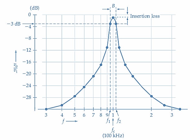
Figure 3. Gain/frequency response graph for the series-resonant bandpass filter in Example 2. Image used courtesy of Amna Ahmad
Parallel Resonant Bandpass Filters
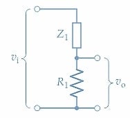
A bandpass filter using a parallel resonant circuit is shown in Figure 4. In this case, the output voltage is developed across the resonant circuit.
\[\frac{v_{_o}}{v_{_i}}=\frac{Z_{1}}{R_{1}+Z_{1}}\,(5)\]
At frequencies above and below resonance, Z1 becomes smaller than R1, so the output is smaller than the input. For a parallel LC circuit, Z1 is a maximum at the resonance frequency (larger than R1), so vo is smaller than vi. The shape of the frequency response for the parallel-resonant bandpass filter is similar to that of the series-resonant filter. The center frequency is calculated exactly as the series-resonant bandpass filter, but the bandwidth must be determined using the parallel circuit Q factor, which is the Q factor of the inductor. There are also differences (between series and parallel resonant bandpass filters) in the circuit attenuation at the resonance frequency and frequencies outside the passband.
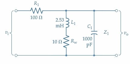
Figure 4. Parallel-resonant bandpass filter circuit. Input voltages are divided across the resistor (R1) and the parallel LC circuit impedance (Z1). Z1 is a maximum at the resonance frequency, so input voltages are passed to the output with little attenuation. Z1 becomes quite small at frequencies above and below resonance, causing inputs with off-resonance frequencies to be severely attenuated. Image used courtesy of Amna Ahmad
Example 3
The parallel resonant bandpass circuit in Figure 4 uses the same component values as the series-resonant filter in Example 2. Determine the resonance frequency, bandwidth, and insertion loss at resonance.
Solution
From Example 2, fr=100kHz
Q factor
\[Q_{P}=\frac{2\pi f_{r}L_{1}}{R_{W}}=\frac{2\pi\times100kHz\times2.53mH}{10\Omega}=159\]
Bandwidth
\[B=\Delta f=\frac{f_{r}}{Q}=\frac{100kHz}{159}=629kHz\]
Impedance
\[Z_{1}=\frac{L_{1}}{C_{1}R_{W}}=\frac{2.53mH}{100pF\times10\Omega}=253k\Omega\]
Insertion loss
\[\frac{v_{_o}}{v_{_i}}=\frac{Z_{1}}{R_{1}+Z_{1}}=\frac{253k\Omega}{253k\Omega\times10\Omega}=0.9999\]
\[Insertion\,loss=20log\Big(\frac{v_{_o}}{v_{_i}}\Big)=20\,log\,log\,0.9999\approx-0.87\times10^{-3}dB\]
Comparing the results obtained in Examples 2 and 3, the parallel-resonant bandpass filter bandwidth is smaller than the series-resonant filter using the same components. The parallel-resonant filter has virtually zero insertion loss, while the series-resonant filter has a loss approaching 1 dB. As already discussed, the series-resonant bandpass filter effectively has infinite attenuation at frequencies well above and below the passband. For the parallel-resonance circuit at very low frequencies, XC1 becomes very large, XL1 is quite small, and Z1RW. Thus, at low frequencies, the signal attenuation is limited to a minimum of,
\[\frac{v_{_o}}{v_{_i}}=\frac{R_{W}}{R_{1}+R_{W}}\,(6)\]
At frequencies above the passband, XL1 increases, and XC1 becomes smaller as the signal frequency increases. Consequently, the attenuation approaches infinity, just as in the case of the series-resonant bandpass filter.
Takeaways of Bandpass Filters
Bandpass filters are essential components in electronic circuits that allow a specific range of frequencies to pass through while attenuating others. Bandpass filters can effectively isolate the desired frequency range using the high-pass, low-pass combination technique. Additionally, series resonant and parallel resonant bandpass filters offer alternative methods for achieving the desired frequency response, providing flexibility in designing circuits for specific applications.