Facebook
 Google
 GitHub
 Linkedin
Case Study—A Low-Cost, Low-Profile 6-kW, 800 V to 12.5 V DC-DC for AI Power
Learn how GaN technology enables a low-cost, low-profile 6 kW, 800 VDC to 12.5 VDC converter using an ISOP LLC topology. This meets the design needs of next-gen, MW-scale AI server infrastructure.
Article co-authored by EPC’s Alejandro Pozo Arribas.
Artificial intelligence is now in vogue - and its influence will only continue to grow. Today, the real challenge lies in delivering the energy demands at optimal efficiency levels. NVIDIA recently released a white paper¹ showing that an 800 V DC architecture combined with energy storage solutions represents an alternative approach to meeting the needs of modern and future AI server infrastructures.
These systems will require power delivery in megawatts, not just kilowatts. The enabling technology is GaN. In collaboration with NVIDIA, EPC has developed a cost-effective, low-profile 800 VDC-to-12.5 VDC converter2 capable of delivering up to 6 kW. The design leverages EPC’s latest 150 V and 40 V GaN device3,4, fitting within a footprint of 5,000 mm² and a total thickness of only 8 mm.
The design exemplifies how GaN FETs can achieve a combination of high efficiency and high power-density while keeping costs low, aiming to achieve 97% efficiency at full load.
The Server Electrical Infrastructure
Current artificial intelligence systems rely on four stages of power conversion - from the AC power grid down to the core voltage - within the same rack that houses GPUs and CPUs. The first two stages, converting AC to 400 VDC and then 400 VDC to 54 VDC, are integrated into power supply units alongside battery backup systems, typically located in dedicated power shelves. The 54 VDC rail is then distributed along the racks to the processing section, where the final two stages step down the voltage from 54 VDC to 6 or 12 VDC and, ultimately, from 6 or 12 VDC to the core voltage (Figure 1).
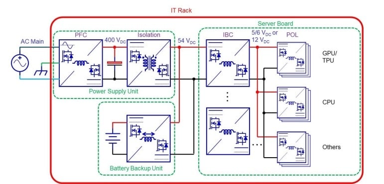
Figure 1. Typical kilowatt server rack architecture2
Today’s GPU racks consume up to 100 times more power than regular web servers1. Because of this exponential growth, thermal design power of processors has increased by 75% and computing performance has gone up by 50%. NVIDIA's white paper1 states that NVLink technology, which lets multiple GPUs work together as a single computing unit, is a big reason for this increase in performance.
The advent of NVLink is driving the total power of the rack to approach 1 MW. To meet this power demand, space within the rack has become premium and thus the proportion allocated to the power supply needs to be adjusted appropriately. This is where the direct 800 VDC to 12.5 VDC architecture stands out, as it is possible to shrink the area and thickness of this power stage to fit within the confines of the GPU rack.
The 800 V Architecture
As data center power needs accelerate, 800 VDC is emerging as the most effective architecture for next-generation distribution, offering clear advantages over traditional 415/480 VAC or 54 VDC approaches. Operating at a higher voltage enables significantly more efficient power transmission for the same cable cross-section, reducing current, copper requirements, and cable bulk throughout the facility. An 800 VDC to 12.5 VDC architecture also streamlines the entire power path.
Fewer conversion stages are required between the grid and the GPU level, which cuts down on cables, connectors, and components while freeing valuable rack space and reducing system complexity. Safety is enhanced through the use of touch-safe connectors and mechanical interlocks - technologies already proven in the EV charging ecosystem.
The transition is further supported by the growing maturity of wide bandgap power devices and by the widespread adoption of 800 VDC in electric mobility. Together, these elements enable a clean, efficient, and scalable end-to-end power distribution model capable of supporting power requirements well beyond 1 MW1.
Also, using a GaN-based LLC converter to go directly from 800 VDC to 12.5 VDC makes the system more efficient and cuts the footprint by about 26%1. This architecture sends 800 VDC directly to the AI racks and then converts it to 12.5 VDC for the point-of-load (PoL) converters that power CPUs and GPUs. Placing the conversion stage close to the load cuts down on bus losses and does away with the 54 V-to-12 V stage that is common in kilowatt-class systems today. This change also makes more room on the rack for high-density computing modules (Figure 2).
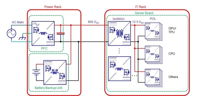
Figure 2. New megawatt-scale power distribution system2
The choice to use a single-ended 800 VDC configuration is based on practical reasons, such as the availability of protection devices and the ease of data center-level distribution. This topology works with standard two-pole switchgear designs, doesn't cause load-balancing problems, and makes deployment faster. The switch to 800 VDC power delivery is not completely new; it builds on improvements in both telecommunications, industrial and automotive systems.
GaN Technology
GaN (gallium nitride) technology is a key factor that makes it possible to use 800 VDC architectures. Compared to traditional silicon devices, GaN semiconductors switch faster, dissipate less power when conducting, and work better at high temperatures. This combination is very important for achieving high power density and efficiency that 800 VDC systems demand.
GaN devices also work at higher switching frequencies, which makes it easier to optimize PCB design and makes passive components like inductors and transformers smaller. This is important for saving space, which is becoming more valuable near GPUs.
The ISOP Solution
A 6 kW, 800 VDC to 12.5 VDC converter that supports 800 VDC power distribution in an artificial intelligence infrastructure, using an LLC topology in an input-series, output-parallel (ISOP) configuration, with high efficiency was designed by EPC2.
The ISOP configuration uses a modular approach in which the input voltage and output current are divided into eight blocks, where each module thus receives only ⅛th of the input voltage and delivers ⅛th of the output current. As a result, the original specification of the 800 VDC to 12.5 VDC converter (64:1 conversion ratio) is reduced to a much simpler 100 VDC to 12.5 VDC (8:1 ratio) with a nominal output power of 750 W per module.
Each module is configured with a GaN FET-based half-bridge power stage powering the primary of a 4:1:1 turns ratio transformer with a center-tapped secondary with GaN FET synchronous rectifiers. This transformer is convenient because it can be constructed as a planar PCB structure. The center-tapped secondary has the added advantage of requiring only one device in the high-current path for the rectifier instead of two in series compared to when using a full-bridge rectifier. Figure 3 displays the block diagram of the ISOP converter and the topology of the 100 VDC to 12.5 VDC LLC module.
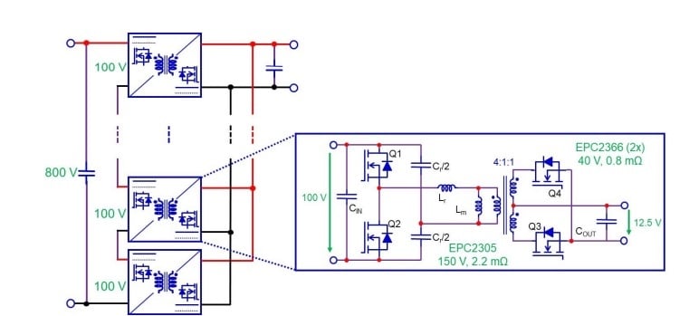
Figure 3. 800 VDC to 12.5 VDC ISOP Converter showing details of the LV module2
LLC Configuration
A half-bride LLC converter minimizes the number of active FETs and gate drivers required, keeping costs low. The turns ratio in the transformer is also reduced by half, simplifying its design considering that it has to have safety isolation built in. Conversely, the RMS current on the primary side of the transformer is twice as high, requiring components with low on-resistance, such as EPC2305. Similarly, a center tap rectifier topology for the secondary reduces the number of active rectifiers and drivers, also contributing to a low-cost solution.
The 12.5 V output value is achieved thanks to the overall conversion ratio of the module. Each module, which receives approximately 100 V at the input, applies a voltage of approximately half the input (50 V) to the primary of the transformer via the half-bridge. With a transformer turns ratio of 4:1, the resulting voltage on the secondary is approximately 12.5 V. Finally, the outputs of all modules, which are connected in parallel, provide a common 12.5 V high-current bus for the load.
The LLC is designed so that the switching frequency operates close to the resonant frequency of the tank, where the tank gain is unity. This means that at the resonant frequency, the tank output voltage is almost equal to the input voltage, with minimized losses and maximum efficiency.
Tank Gain Independent of Operating Frequency
By designing Lᵣ much smaller than Lₘ (Lᵣ << Lₘ), the tank gain becomes independent of the operating frequency over a wide range and stabilizes the voltage conversion. This ensures that the parallel outputs give each of the primaries the same voltage, ensuring that the 800 VDC input is evenly divided across all of the modules5.
Low-voltage GaN devices can be employed on the primary side and have much better figures of merit than 1200 V SiC or 650 V GaN FETs6.
In addition, the eight LLC modules that constitute the ISOP configuration can have their switching cycles interleaved to reduce input/output voltage ripple, minimizing bus capacitance requirements.
EPC's implementation of this solution operates each module at 1 MHz switching frequency, which allows for a tiny, low-profile core with a thickness of 5.8 mm. This thickness is critical, as it keeps the overall solution within 8 mm of total thickness. As a result, it can be cooled without interfering with the processor’s cooling system.
The EPC23053 is the logical choice for the primary side with a typical RDS(on) of 2.2 mΩ and a gate charge QG of 22 nC. The output charge QOSS is only 103 nC with QRR = 0 (no reverse recovery typical of GaN), resulting in a soft-switching figure of merit7 of 275 mΩ·nC. The 3×5 mm QFN package with exposed substrate option offers a junction-to-case thermal resistance of 0.2°C/W.
On the secondary side, two parallelled EPC23664 provide a combined RDS(on) of 0.4 mΩ with a total gate charge QG of 26 nC, and QOSS of 40 nC. Each device comes in a 2.6×3.3 mm QFN package with exposed substrate and thermal resistance of 0.6°C/W.
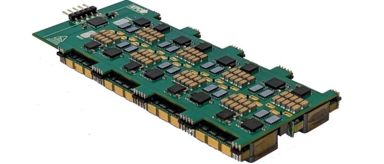
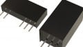
Figure 4. Photo of the EPC91123, 6 kW, 800 VDC to 12.5VDC, Demo Board2
Conclusions
The 6 kW, 800 VDC-to-12.5 VDC ISOP converter from EPC shows how GaN technology can be used to make modern AI server infrastructures that are both high-efficiency and high-power-density (figure 4). The modular LLC design ensures low losses, high efficiency, and a compact footprint.
Leveraging EPC’s mature GaN technology, the system achieves close to 98% peak efficiency and 97% full load efficiency while supporting megawatt-scale power densities. This approach exemplifies the future of AI power delivery, bridging the gap between emerging data center demands and practical, scalable electrical designs.
All images used courtesy of EPC (Efficient Power Conversion).
References
[1] White Paper, 800 VDC Architecture for Next-Generation AI Infrastructure - Jared Huntington & Mike Tu, Nvidia
[5] Q. Ma, Q. Huang and A. Q. Huang, "Zero-Voltage Switching and Natural Voltage Balancing of a 3 kW 1 MHz Input-Series-Output-Parallel GaN LLC Converter," in IEEE Open Journal of Power Electronics, vol. 5, pp. 1119-1128, 2024, doi: 10.1109/OJPEL.2024.3433562.
[6] A. Pozo and M. A. de Rooij, "5.5 kW Isolated 400 V to 50 V DC-DC Converter for Server Power Supplies," PCIM Conference 2025; International Exhibition and Conference for Power Electronics, Intelligent Motion, Renewable Energy and Energy Management, Nürnberg, Germany, 2025, pp. 637-645.
[7] A. Lidow, M. de Rooij, J. Glaser, A. Pozo, S. Zhang, M. Palma, D. Reusch, and J. Strydom, “GaN Transistors for Efficient Power Conversion”, 4th ed. John Wiley & Sons, 2025. ISBN: 978-1394286959