Facebook
 Google
 GitHub
 Linkedin
Understanding the Behavior, Circuit Design, and Variants of Ćuk Converters
Learn about the physics behind the operation of Ćuk converter topology, design insights, and an overview of its variants.
In "What is a Ćuk Converter?" we learned about what DC-DC converters are and how they find applications in a wide array of fields. We also studied a variant of the buck-boost converter called the Ćuk converter that effectively steps-up or steps-down the voltage at different time instants based on the requirement. Read on to learn more about the physics behind the operation of Ćuk converter topology, design insights, and an overview of its variants.
The Physics Behind a Ćuk Converter Circuit’s Behavior
The initial hardware implementation of a Ćuk converter was accomplished using the diode transistor combination forming the ideal single-pole double-throw switch [1]. Observing the circuit in Figure 1, it is evident that the coupling capacitor is charged due to the input current flowing when the switch is turned off and the diode is on or forward biased.

Figure 1. Circuit diagram of the Ćuk converter
Similarly, when the switch is conducting, the voltage across the coupling capacitor reverse biases the diode thus turning it off and the stored charge in the coupling capacitor is discharged through the switch to the load. This explains the crucial capacitive energy transfer concept which is the basis for this specific converter topology.
Traditionally, converters operate based on the inductive energy transfer like in the buck, boost, and buck-boost topologies. Again, observe the circuit diagram and notice that the unique non-pulsating terminal currents are possible due to the presence of two inductors in series with the input and output ports.
Insights for Designing and Realizing a Ćuk Converter
A Ćuk converter can be considered a conventional buck converter preceded by an input filter. This means that the design criteria with respect to dynamic performance can be adapted to provide a four-pole input to output transfer function along with a two-pole control to the output transfer function. In simple terms, design can be implemented by choosing suitable relative corner frequencies and the damping of the effective input and output filters inherent in the Ćuk converter.
The first set of parameters can be chosen based on the input and output specifications. If there is an additional isolation transformer included in the conventional topology, the choice of scaling ratio is governed by the duty ratio requirement for the given output and line input voltages.
The minimum values of inductors and capacitors can be determined based on the current and voltage ripple considerations. For instance, a larger value of voltage ripple on the capacitors increases the voltage stress on the switch and the diode. Along those same lines, a large value of the current ripple in the inductor increases the current stress on the switching device and the diode while raising the minimum load current.
The chosen first set of parameters mostly based on the switching frequency and stress considerations explained before might not be suitable when the sc dynamics of the converter are accounted for. In such cases, the dynamic properties can be represented using a linear, small-signal canonical model of the Ćuk converter just like it is done for other converter topologies.
The parameters are all reflected on one side of the converter, preferably the output side to form the linearized small-signal model. Conversion ratios can be chosen based on the approximation of cent percent efficiency. The resulting circuit provides insight into parameter selection as it accounts for both DC and small-signal AC properties of the converter.
Topologies Derived from the Conventional Ćuk Converter
The two individual inductors present in the conventional Ćuk converter can be coupled and wound on the same core resulting in the coupled inductor based topology. The transformer-like action or the mutual inductance control inside the coupled component translates to enhanced ripple reduction either on the input or the output side, based on the design considerations.
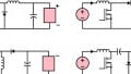
The addition of a transformer and a capacitor converts the conventional non-isolated Ćuk converter to an isolated topology often referred to as integrated magnetics based topology. The process of obtaining isolation is illustrated in Figure 2.

Figure 2. Obtaining an isolated version of the conventional Ćuk converter
In this case, the inductors and the transformer windings can be wound on the same core thus reducing the losses, cost, and size, while enhancing the performance and power density. The turns ratio provides additional control during the design so that device stress can be reduced on the input side.
Pros and Cons of Other Buck-Boost Topologies Used for Similar Applications
In general, variants of the buck-boost converter like Ćuk, SEPIC, and Zeta converters are derived based on the interconnection of several buck converters and boost converters in cascade or cascode form [2]. A traditional buck-boost topology can be used to increase or decrease the input voltage. They comprise a single inductor and capacitor, making them cheaper than the other topologies listed below. Some applications require only buck or boost operation and in such cases, only the specific converters can be utilized.
A single-ended primary-inductance converter (SEPIC) is another variant of a buck-boost converter with the ability to increase or decrease the input voltage by controlling the duty cycle of the pulse to the switching device. It can be implemented using minimal active components and a simple controller. Although this control method is suitable, it can be insufficient for several critical applications.
The Zeta converter is similar to the SEPIC converter topology. It provides a positive output voltage. In this case, the input voltage varies above and below the output voltage. It comprises two inductors and a series capacitor usually referred to as a flying capacitor thus involving a high number of passive elements. Also, the input current is discontinuous, making it unsuitable for some of the applications.
Key References
- Slobodan Ćuk and R.D.Middlebrook, Advances in Switched-Mode Power Conversion, TESLAco, Vol II.
- Robert W Erickson and Dragan Maksimovic, Fundamentals of power electronics, Springer Science & Business Media, 2007.