Facebook
 Google
 GitHub
 Linkedin
Reverse Conducting IGCT Platform optimized for Modular Multilevel Converters MMC
This article discusses the technical aspects of ABB's newly developed Reverse Conducting Integrated Gate Commutated Thyristor (RC-IGCT) platform.
ABB has developed a new Reverse Conducting Integrated Gate Commutated Thyristor (RC-IGCT) platform and recently the first products such as the 4.5kV / 3kA and a 6.5kV / 2.15kA RC-IGCT have reached the production stage. The development was driven by high voltage converters for STATCOM applications with Multi-level Modular Converter (MMC) topology. The IGCT was chosen because of the low switching frequency with subsequent potential for low losses, as well as the straightforward inclusion of redundant cells for continuous operation after faults.
Performance / On-state
In an MMC application with comparably low switching frequency, the on-state losses are crucial for the system’s efficiency. This is one of the most important advantages of the IGCT over the IGBT for this type of application.
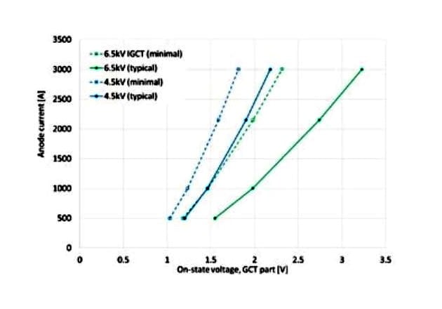
Figure 1: IGCT on-state voltages for the 4.5kV and 6.5kV IGCTs. The "minimal" curves are what can be achieved without reducing the carrier lifetime
Thermal
Figure 3 shows a simulation of the thermal response of the developed RC-IGCT compared to the existing platform, at the same power level and using the same color scale for the temperature. The new housing omits the pole-piece trenches needed for conveying the gate signal, and those that incorporate the gate spring system over the active area. This has a profound effect on the maximal junction temperature and especially on surge-current capability. Additionally, the wafer was shifted from the axial center of the package, closer to the anode thermal contact which reduces RTH for the device in general.


Figure 2: Output of thermal simulations of the existing (top) and new (bottom) RC-IGCT technology at identical power density in the active parts. The maximal silicon temperature is 30°C lower using the newly developed package. The color scale indicates the temperature in °C. The heated (reddish) parts is the silicon device, stacked with molybdenum disks and copper pole-pieces. The cathode sides are directed upwards. Both devices are stripped of thermally irrelevant features, such as flanges, rubber, plastic and ceramic parts.
Maximal controllable current
The HPT+ platform was incorporated in the new RC-IGCT for improving the high-temperature current controllability. Together with the improvements in gate-circuit impedance – it was reduced by more than a factor of three – the current-handling capability of the system could be significantly improved. Both the diode and GCT parts can be switched much beyond the SOA-specification at 135°C as shown in Figure 3. At lower junction temperatures, the maximum controllable current increases to over 6 kA.

Figure 3: Sample waveforms from a 4.5kV RC-IGCT, switching OFF above 4500A at 3.2kV DC-Voltage
The diode is extremely robust. It is governed by the current rate of change during reverse recovery. In IGCT applications, the dI/dt is moderated by dimensioning a reactor together with the maximal cell voltage. For an appropriate selection of cell DC voltage and size of the choke, there is almost no limit to how much forward current the diode can recover from. For these new products, the limit has not even been established exactly, because it so much higher than the specified requirement, that the actual capability is of academic interest only.
Snap-OFF
A challenging task is to ensure nice behavior at low forward current and high cell voltage over the whole temperature range. The most straightforward way to improve the switching behavior is to increase the diode thickness, albeit with obvious loss drawbacks. It is particularly important for RC-IGCTs to minimize the diode thickness, due to the integration of both the switch and the diode on the same Silicon wafer. In order to keep snap-off within acceptable limits at a maximal cell voltage of 3.2kV, it was necessary to use a double proton peak for the 4.5kV device. The 6.5kV device prevailed with the single proton peak, with the maximal cell voltage of 4.6kV.
Reliability
As a new device platform, the devices have successfully passed the full range of accelerated reliability testing such as temperature- and load cycling. Hence, ABB is confident that the newly developed technology platform will display the same excellent reliability track-record as its predecessor.
Application
Including an adequately large number of levels in an MMC system leads to a virtual disconnection of the higher-order harmonic output from the switching frequency of the semiconductors. In theory, this can be as low as the output’s fundamental frequency, which is 50 or 60 Hz in grid applications. In contrast, for inverter topologies with fewer levels, the harmonic content decreases with increased semiconductor switching frequency. The possibility of low switching frequency favored the selection of the IGCT as the inverter’s main switch, thanks to its inherent low on-state voltage compared to the IGBT. Another significant advantage of the hermetic press-pack IGCT is that it can potentially handle large fault currents without rupturing. Hence, choosing the IGCT also facilitated securing the cell integrity, including safety of equipment, at very low extra effort and cost.
Figure 4: The Power-Electronic Building Block containing two MMC cells with four RC-IGCTs each
Design
The existing RC-IGCT platform was developed further as both the size of the diode as well as the current handling capability needed increasing for the intended application. A positive side-effect of platform development is the opportunity to review all design aspects. In that endeavor, it was possible to improve on existing thermal bottlenecks that impede particularly the surge-current capability. One of the basic requirements was maintaining the backwards mechanical compatibility to the existing platform. As a result, the new device is identical on the outside, with the same outer dimensions as its predecessor.
The incorporation of an outer ring gate structure in combination with the integration of HPT+ technology on the RC-IGCT platform addressed both future requirements on current handling capability as well as performance at high junction temperatures. The gate circuit impedance was reduced further by wrapping the gate leads close to the cathode pole-piece. The gate contact was moved to the periphery of the device. The move increases the area consumption of the gate contact infrastructure by necessity, if nothing else is changed. To counteract the loss of active area, the centering tolerance of the gate contact on the wafer was much improved. Thus, despite the new contact has a larger diameter, the space consumption for the gate infrastructure could be reduced. Combined with increasing the maximal device diameter capability of the production facility, the active area could be significantly increased without increasing the size of the raw silicon wafer. All of the active area gain was given to the integrated diode, which almost doubled in size. Nevertheless, the improvements in wafer technology, lowering the gate circuit impedance and removing thermal bottlenecks, the IGCT performance could be improved too, without increasing the size of the IGCT part.
The 4.5kV diode receives local lifetime control in two axial positions; the 6.5kV in just one position, due to the switching behavior at low current and high voltage. The double-position lifetime control has a drawback: it limits the minimal on-state that can be achieved, so it will be a target for future developments to incorporate a different technology, for example, FCE to improve the switching behavior of the 4.5kV device.
Conclusion
A 4.5kV / 3kA and a 6.5kV / 2.15kA RC-IGCT optimized for low-frequency applications, such as grid applications employing the MMC topology. In order to fulfil the requirements, a new technology platform for RC-IGCTs was developed. This platform will serve as the base for future technology large area IGCTs from ABB, also for applications with higher switching frequency.
This article originally appeared in the Bodo’s Power Systems magazine.
About the author
Tobias Wikström has developed power semiconductors for ABB since 2001. As a matter of course, he has specialized on IGCT technology, and was the development project manager for the new RC-IGCT platform until its transfer to production.