Facebook
 Google
 GitHub
 Linkedin
Reduce Costs: Use the Same Qualified Parts for Positive and Negative Output DC-to-DC Converters
One relatively easy way for manufacturers to reduce the cost of electronic components is by using the same designs or components for disparate applications. The cost savings manifest not only in bulk procurement of identical parts but in minimizing the number of required qualification processes.
This article shows how to use the same components—an IC controller and power train—in two very different topologies: a common buck converter and in an inverting buck-boost converter. The component requirements are explored for the inverting buck-boost converter by specifically examining the reverse voltage fluctuation on the output of the inverting buck-boost, and ways to use the least expensive polarized capacitors in this topology. As a result, a simple and cost-effective solution for designing positive buck and negative buck-boost converters using the same IC is presented.
Positive Output, Buck Converter
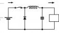
The electrical schematic of the positive output, the buck converter is presented in Figure 1. The converter generates a stable VOUT of 5 V at 15 A from the input voltage VIN range of 5 V to 38 V. The power train includes modulating (high-side) MOSFETs Q1 and Q2, rectifying (low-side) MOSFETs Q3 and Q4, inductor L1, a combination of the electrolytic and ceramic input filter capacitors CIN1 and CIN2, and a similar combination of capacitors for the output filter and the controller.
The resistor RS can be used as a current-sense element if the peak current mode controller is employed, or as part of the short-circuit protection circuitry in voltage mode control. The input capacitors CIN1 and CIN2 are terminated to GND; however, the optional CIN3 and CIN4 are terminated to the output and are employed in the negative buck-boost solution. The functionality of buck converters is widely studied and easily obtainable. In this article, we just briefly note voltage and current stress on the power train components. It is relevant to the preliminary selection of components in new designs and rough evaluation of the existing solutions. Assuming continuous conduction mode (CCM) operation, the following expressions can be used.
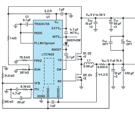
Figure 1. Electrical schematic of a step-down, buck converter with VIN 5 V to 38 V, and VOUT 5 V at 15 A. Image used courtesy of Bodo’s Power Systems [PDF]
\(D=\frac{V_{OUT}}{V_{IN}}\) Duty cycle
\(V_{DS}=V_{IN}\) Maximum voltage stress on Q1 through Q4 and LI
\(I_{L}=I_{OUT}+0.5\times \Delta I\) Inductor L1 peak current, where ΔI is peak-to-peak ripple current.
Negative Output, Negative Buck-Boost Converter
The schematic of the negative buck-boost converter presented in Figure 2 is similar to the buck converter schematic in Figure 1. Notably, both use the same components for the power train, interconnections, and controller. Differences arise in the grounding of the controller, switching MOSFETs, and input/output filter. The ground of these inverting converter components is –VOUT. The inductor L1 is terminated to the system (input) ground.
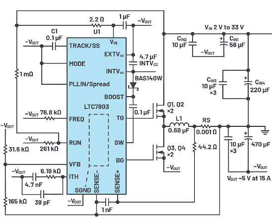
Figure 2. Electrical schematic of an inverting buck-boost converter with VIN 2 V to 33 V, VOUT –5 V at 15 A, and start-up input voltage +5 V. Image used courtesy of Bodo’s Power Systems [PDF]
Unlike in the buck converter, the capacitors CIN3 and CIN4 are not optional in this solution; they function as the input filter. The capacitors CIN1 and CIN2 filter ac between the VIN and –VOUT rails. The following expressions can be used to estimate the stresses on the power train components, assuming CCM operation.
\(D=\frac{|V_{OUT}|}{V_{IN}+|V_{OUT}|}\) Duty cycle
\(V_{DS}=V_{IN}+|V_{OUT}|\) Maximum voltage stress on Q1 through Q4 and LI
\(I_{L}=\frac{I_{OUT}}{1-D+0.5\Delta I}\) Inductor L1 peak current, where ΔI is peak-to-peak ripple current.
Converter Functionality and Testing
There’s plenty of literature covering the basic and even advanced functionality of these two types of converters.1 In the remainder of this article we’ll examine rarely discussed factors.
First, there is a fundamental difference in functionality of the output filters between the buck and buck-boost topologies. In the buck configuration, the inductor is hardwired to the output filter, providing continuous output current in CCM. Unlike the buck, the buckboost topology does not connect the inductor only to the output. During the Q1/Q2 on-time, the inductor L1 is disconnected from the output filter and the output filter capacitance is the only source of energy to the load. Consequently, it’s important to have enough output capacitance to absorb the discontinuous output capacitor current and support the specified output voltage ripple.
There is a drawback in negative buck-boost and, in fact, most inverting topologies. At startup there is a reverse voltage swing at the output filter with amplitude not more than one diode voltage drop, as shown in Figure 3. This brief reverse voltage is due to the flow of the controller’s operating current through the forward-biased diode to system ground. The existence of the reverse voltage on polarized capacitors appears unacceptable at first glance. Hence, some designers eliminate polarized capacitors from the output filter, resorting to ceramic-only capacitors. This approach creates other problems associated with the size, cost, and dc bias of the ceramic capacitors. Nevertheless, it is possible to use polarized capacitors in inverting buck-boost applications with some limitations. The guidelines vary by vendor—an example of such recommendations can be found in Polymer, Tantalum, and Niobium Oxide Capacitors: Application Guidelines.2
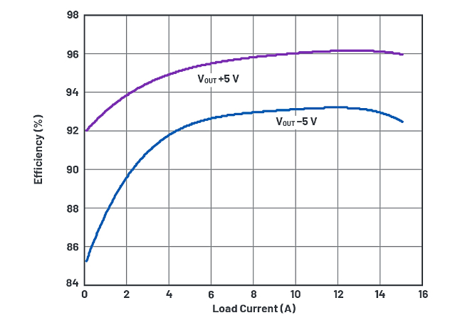
Figure 4. Efficiency of the converters in Figure 1 and Figure 2 (VIN 12 V, natural convection cooling, no air flow). Image used courtesy of Bodo’s Power Systems [PDF]

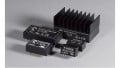
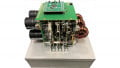
Figure 5. DC2834A converted to inverting buck-boost from the original, off-the-shelf step-down converter. Image used courtesy of Bodo’s Power Systems [PDF]
The converters shown in Figure 1 and Figure 2 were thoroughly tested and evaluated. Their efficiency is shown in Figure 4. To simplify the design with a low pin count and wide input voltage range, making it applicable to a wide variety of solutions, the LTC7803 advanced controller was used in both cases. The evaluation board DC2834A was used as a basis (with some modification) to verify both applications. To reduce EMI, the spread spectrum feature of this controller can be employed. Figure 5 shows a photo of the buck DC2834A converted to inverting buck-boost.
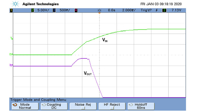
Figure 3. An inverting buck-boost converter with start-up waveforms. Channel 2’s VIN is 5 V/div, while Channel 3’s VOUT is 0.5 V/div with a 2 ms/div timescale. Image used courtesy of Bodo’s Power Systems [PDF]
Conclusion
This article presents a way to use the same controller and a number of identical components for positive step-down and negative buck-boost converters. In this way, costs for qualifying components can be reduced. Costs can be further reduced by using a controller that requires a minimal number of power train components and supports synchronous rectification, resulting in efficient, low EMI, wide input voltage range solutions.
This article originally appeared in Bodo’s Power Systems [PDF] magazine.
Featured image used courtesy of Adobe Stock