Facebook
 Google
 GitHub
 Linkedin
Preventing Under and Overdamping With Optimized GaN Gate Switching Waveforms
Discover how optimizing gate resistance and adding RC snubber networks can effectively suppress gate voltage oscillations and overshoots during GaN HEMT switching.
This article is published by EEPower as part of an exclusive digital content partnership with Bodo’s Power Systems.
Enhancement-mode GaN HEMTs feature fast switching speed, low on-resistance, and high power densities. As such, they are ideally suited for use in high-frequency, high-efficiency power conversion and RF circuits. However, due to their small gate capacitance, low gate threshold voltage (typically between 1V and 2V), and limited voltage tolerance (usually -5V to 7V), steps need to be taken to prevent device failure through unintended turn-on and oscillation during switching. In particular, special attention must be paid to the gate driver.
This article seeks to address this challenge by providing an in-depth analysis of the oscillation mechanisms in GaN HEMTs during turn-on and turn-off. It also demonstrates how strategies, such as proper gate resistance configuration and the addition of an RC damping network between gate and source, can be deployed to effectively suppress oscillations and overshoot.

Image used courtesy of Freepik
During testing for the article, validation of optimization results under various device and parameter combinations has been undertaken using the NOVOSENSE NSD2622N high-voltage half-bridge GaN HEMT driver, which has enabled a stable and reliable high-frequency driver design to be used.
Oscillation Mechanisms and Driver Design Considerations in GaN HEMT Switching
A typical GaN HEMT driver circuit can be seen in Figure 1, with resistors R1 and R2 used to respectively adjust the turn-on and turn-off speeds. The driver loop can be regarded as a series LRC circuit, and during turn-on, the gate voltage may exhibit oscillations or overshoots due to the high drain dv/dt, the Miller capacitance (CGD), and the current path illustrated as Isrc.
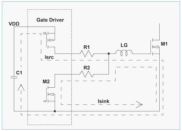
Figure 1. GaN HEMT Driver Circuit. Image used courtesy of Bodo’s Power Systems [PDF]
In this, excessive oscillations or overshoots can, at best, increase GaN HEMT power loss or, at worst, cause device failure. To prevent this, we need to consider the total equivalent parasitic inductance during turn-on (LG), and the equivalent gate capacitance of the GaN HEMT (CGS), with the following formula used to calculate the minimum total equivalent gate resistance during turn-on (RG(eq)):
\[R_{G(eq)}\geq2\times\sqrt{\frac{L_{G}}{C_{GS}}}\]
Similarly, the gate voltage may experience excessive negative overshoot or oscillation during turn-off, with this caused by parasitic inductance in the driver loop and the gate turn-off speed. Here, the result is gate breakdown or false turn-on, with the current path in Figure 1 shown as Isink. Again, special attention should be paid during design to prevent these potentially catastrophic side effects.
As can be observed in Figure 1, the current paths Isrc (turn-on) and Isink (turn-off) differ, which results in different total equivalent parasitic inductances and resistances. More specifically, during turn-on, LG includes parasitic inductance from the power supply path, whereas during turn-off, LG does not. This distinction must be considered during analysis and calculation.
Methodology
To better understand the influence of different gate drive resistors on GaN HEMTs, validation tests are conducted using the NSD2622N dual-channel half-bridge GaN HEMT driver from NOVOSENSE in conjunction with two different GaN HEMTs. The tested devices and corresponding results are briefly described below.
NOVOSENSE NSD2622N is a high-voltage half-bridge GaN HEMT driver in a 5x7 mm QFN package. Its functional block diagram and pin definitions are shown in Figure 2 and Figure 3, respectively, and the device adopts mature capacitive isolation technology, which enables it to meet the requirements of high-voltage applications. Both its high- and low-side drivers integrate dedicated positive/ negative voltage regulators to provide adjustable positive voltage from 5V to 6.5V and a fixed negative voltage of -2.5V, ensuring reliable negative-voltage turn-off for GaN HEMTs.
The driver features low propagation delay and high drive current (peak source/sink currents of 2A/-4A), satisfying the requirements of diverse systems. It also provides undervoltage lockout (UVLO), over-temperature protection, and dead-time interlock capabilities. It should be noted that the dead-time interlock function can effectively prevent shoot-through in bridge-leg configurations. Additionally, the driver provides a 5V LDO output, offering greater system design flexibility.
Additionally, two high-voltage GaN HEMTs in TOLL packages with Kelvin source pins were used in the validation tests: INNO65TA080BS and GS0650306LL. Key parameters for these devices are listed below.
A double-pulse test setup, as shown in Figure 4, was used to measure gate waveforms of the GaN HEMTs under different gate resistances. The drive loop reference ground of the HEMT driver was connected to the GaN HEMT Kelvin source pin.
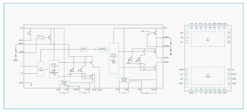
Figure 2. NSD2622N Functional Block Diagram and Pin Definitions. Image used courtesy of Bodo’s Power Systems [PDF]
The total parasitic inductance of the gate drive loop during turn-on was approximately 38nH. Using the CISS value from the GaN HEMT datasheet, the equivalent gate resistance RG(eq) during turn-on should be no less than 26Ω. To directly observe the effects of underdamping, R1 values of 10Ω and 27Ω were tested. The measured waveforms for each of these variables can be seen in the table below, with the blue trace representing the GaN HEMT drain voltage, the green being the inductor LM current, and the yellow being the GaN HEMT gate voltage.
Table 1.
|
Parameter |
INNO65TA080BS |
GS0650306LL |
Unit |
|
VDS |
650 |
700 |
V |
|
ID |
29 |
40 |
A |
|
VGS |
-6~7 |
-10~7 |
V |
|
Vth |
1.7 |
1.7 |
V |
|
RDS(on) |
60 |
40 |
mΩ |
|
CISS |
225 |
235 |
pF |
|
COSS |
70 |
70 |
pF |
|
CRSS |
0.5 |
1.6 |
pF |
|
QRR |
0 |
0 |
nC |
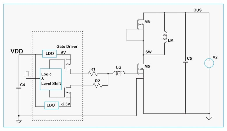
Figure 3. Double-Pulse Test Setup. Image used courtesy of Bodo’s Power Systems [PDF]
As we can see, when R1 = 10Ω, the turn-on drive loop operates in an underdamped mode. At a bus voltage of around 50V, both GaN HEMTs exhibit high-frequency oscillations in gate and drain voltages, rendering the system inoperable.
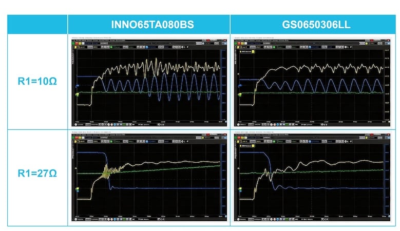
Figure 4. Measured waveforms at 10Ω and 27Ω. Image used courtesy of Bodo’s Power Systems [PDF]
Conversely, when R1 = 27Ω, both GaN HEMTs operate normally at 400V, but INNO65TA080BS exhibits severe high-frequency oscillation in gate voltage during turn-on. This primarily results from differences in parasitic inductance of the internal source and di/dt during turn-on between the two GaN HEMTs, which leads to distinct gate ringing characteristics.
To mitigate such oscillations, we both increased R1 to 33Ω, and implemented an RC snubber (20Ω + 1nF) in parallel between the gate and source. These two methods both reduced the turn-on speed of GaN HEMTs and di/dt during turn-on, and the corresponding waveforms can be seen below.
As we see in Figure 5, at a 400V bus voltage, both adjustment methods enable normal operation, with significantly improved gate voltage oscillation and overshoot. Compared with simply increasing R1, connecting an RC snubber in parallel between the gate and source results in a smoother gate voltage without obvious overshoot, but with longer turn-on delay and increased power dissipation. This should be taken into consideration during design.
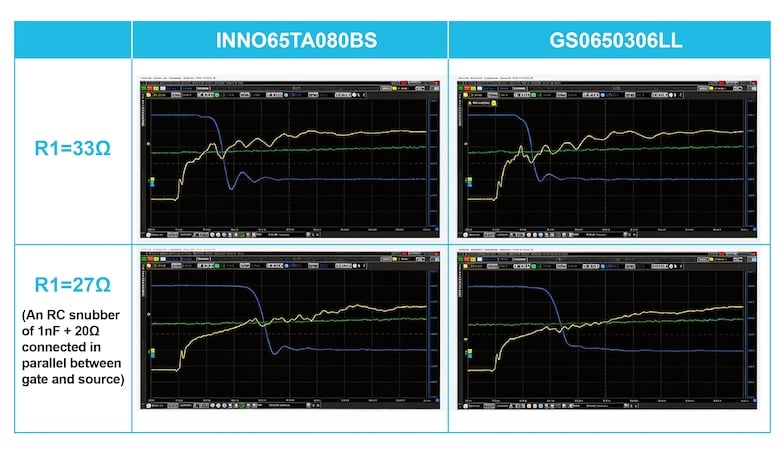
Figure 5. Turn-On Waveforms After Parameter Adjustment. Image used courtesy of Bodo’s Power Systems [PDF]
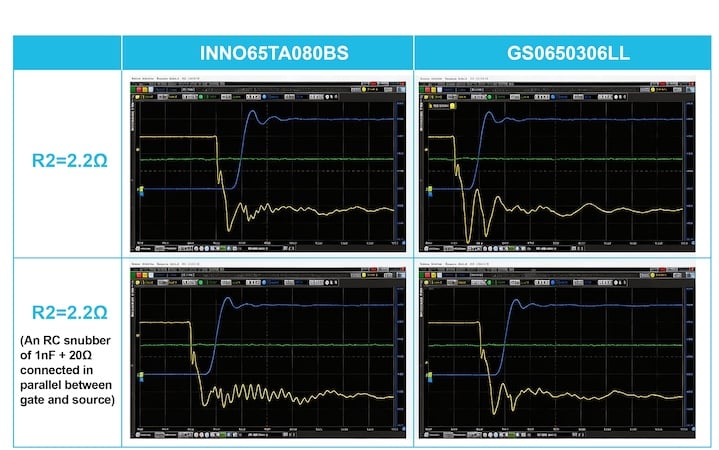
Figure 6. Gate Waveforms During Turn-Off. Image used courtesy of Bodo’s Power Systems [PDF]
From Figure 6, we can also see that during negative-voltage turn-off, significant negative overshoot and oscillation occurred at the gate, but no false turn-on was observed.
When the RC snubber is absent, the negative overshoot exceeded -5V. After adding the RC snubber, the amplitude of negative overshoot was clearly reduced. The negative overshoot and oscillation during turn-off can be further optimized by adjusting the value of resistor R2 or the RC snubber parameters.
Conclusions and Recommendations
Test results confirm that proper gate drive resistance ensures stable and reliable operation of GaN HEMTs. They also highlight that excessively small gate resistance can easily lead to gate voltage oscillation, and with it the potential for system malfunction or failure. Therefore, for enhancement-mode GaN HEMT driver design, the gate drive resistance needs to be tightly defined to prevent gate-source voltage overshoot and oscillation during turn-on, using the equation:
\[R_{G(eq)}\geq2\times\sqrt{\frac{L_{G}}{C_{GS}}}\]
When calculating LG, parasitic inductances from both PCB traces, as well as the chip, in the driver loop should be taken into full consideration. For different GaN HEMTs, an appropriate RC snubber can be connected in parallel between the gate and source to effectively suppress oscillation spikes during switching. For high-voltage GaN HEMTs, negative-voltage turn-off can also prevent unintended turn-on during turn-off. Additionally, the driver ICs should be placed as close as possible to the GaN HEMT to minimize parasitic inductance in the driver loop, and GaN HEMTs with Kelvin source pins are recommended.
This article originally appeared in Bodo’s Power Systems [PDF] magazine.