Facebook
 Google
 GitHub
 Linkedin
Bi-Directional GaN Switches: Conversion with Single-Stage BDS Converters
A single-stage with bi-directional GaN eliminates the PFC stage and the DC-link capacitors while enabling ultra-high frequencies. What are the implications and benefits?
This article is published by EEPower as part of an exclusive digital content partnership with Bodo’s Power Systems.
Over 70 % of today’s high-voltage power converters use a ‘twostage’ silicon topology. For example, a typical AC/DC EV On-Board Charger (OBC) implements an initial power-factor-correction (PFC) stage and a follow-on DC/DC stage, which is buffered with bulky ‘DC-link’ capacitors. The problem with this topology is that the resulting systems are large, lossy, complex and expensive.
This article looks at a new class of power converter that enables single-stage conversion and allows bi-directional power to move back and forth between storage and the grid as required.
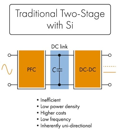
Figure 1. Over 70 % of today’s high-voltage power converters use a two-stage topology, with a PFC stage followed by a DC/DC stage to deliver the desired voltage. Image used courtesy of Bodo’s Power Systems [PDF]
Short History of Bi-Directional Power Converters
An ideal switch is bi-directional, able to block voltage in both directions AND handle current in both directions. It would offer minimal conduction and dynamic losses, dissipate heat effectively, and have a high-power density. In the nearly 80 years since the creation of the bipolar transistor (1947), there have been many developments in power semiconductors that have moved the industry closer to this ideal.
The thyristor (1957) was capable of handling voltage in both directions, but not current. The triac (1958) could handle both current and voltage, but was very slow and operated at just 50 or 60 Hz, matching the AC line. The MOSFET (1959) could operate at tens of kilohertz, even 100 kHz. A bi-directional MOSFET was subsequent created, but this was low power and had limited applications. The silicon IGBT (1980) followed and offered much higher power, but bidirectional functionality remained a challenge, with the IGBT able to handle either current OR voltage, but not both in a single device.
The introduction of wide bandgap semiconductors enabled significant gains in power technology, significantly improving power density; but again, these initial devices lacked bi-directional capability. The use of gallium nitride (GaN) took things further, providing higher switching frequencies and high power, with integrated control and protection on the same chip. However, it still wasn’t bi-directional.
In March, however, Navitas launched the industry’s first bi-directional 650 V GaN power IC, enabling the transition of power conversion from a two-stage, to single-stage topologies. Navitas’s NV6427 and NV6428 are bi-directional GaN power ICs that deliver at 650 VSS continuous with an RSS(ON)typ. of 50 mΩ (ISS of 49 A) and RSS(ON)typ. of 100 mΩ (ISS of 25 A). They have zero reverse-recovery charge and operate at up to 2 MHz. They are housed in a TOLT-16L thermallyenhanced top-cooled package.
Bi-Directional GaN Power Switch
The advent of bi-directional GaN power switch consolidates the two stages into a single, high-speed, high-efficiency stage, and in the process, eliminating the bulky capacitors and input inductors. It is able to handle current and voltage in both directions and switch at very high frequency which means that it is well-suited for singlestage converters.
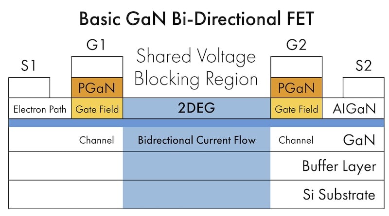
Figure 2. Bi-directional GaN switches use a GaN/AlGaN structure on silicon substrate to create a two-dimensional electron gas (2DEG) conducting channel with two power terminals and two gates. Image used courtesy of Bodo’s Power Systems [PDF]
The bi-directional GaN must handle voltage in both directions and therefore requires separate gates to control current flow depending on polarity. To achieve this, a GaN/AlGaN epi-stack is grown on a silicon substrate to form a 2DEG conducting channel. The processed device structure features two power terminals and two gates. Implementing this structure alone would have performance issues as the silicon substrate is not associated with the source terminals and therefore floats, leading to a substrate potential buildup and reducing the 2DEG concentration due to this ‘back-gating’ effect.
Navitas was the first to develop and release an active-substrateclamp to autonomously drive the silicon substrate to the source with the lowest potential. This has the resulting benefit of enabling the BDS (Bi-Directional Switch) to operate stably with no shifting in resistance and to run 15 °C cooler in many applications than alternative unclamped solutions. This improvement can be seen in Figure 4, with current (green triangle wave), and voltage across the switch: clamped (pink curve) and unclamped (white curve). Here we see proper clamping removes any increases, improving efficiency and enabling a smoother operation.
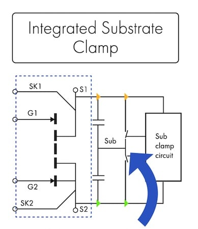
Figure 3. The devices automatically detect and connect alternative sources to substrate. Image used courtesy of Bodo’s Power Systems [PDF]
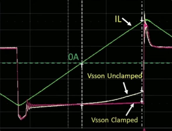
Figure 4. Clamped (pink) / unclamped (white) voltage and current (green) across the switch – with clamped voltage not displaying an efficiency-reducing voltage spike. Image used courtesy of Bodo’s Power Systems [PDF]
It should also be noted that bi-directional GaN also requires a dedicated driver to control its two gates, which must be capable of handling high transient conditions, very high voltage isolation, and ensure exceptional signal integrity. In this case, the device is able to operate at over 5 kV and handles extreme transients up to 200 V/ns.
Therefore, to complement the bi-directional GaN, the IsoFast driver has been developed as a high-speed isolated GaN driver, specifically tailored for this switch, operating at over 1 MHz and handling 5 kV while maintaining high-speed signals with integrity switch, operating at over 1 MHz and handling 5 kV while maintaining high-speed signals with integrity. Additionally, no negative drive is required to turn-off the device, reducing cost and complexity.
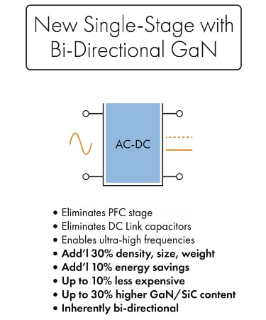
Figure 5. The new singlestage with bi-directional GaN eliminates the PFC stage and the DC-link capacitors while it enables ultra-high frequencies. This means additional 30 % in terms of densitity, size and weight, complemented by 10 % energy savings and up to 10 % of price savings for the system solution. Image used courtesy of Bodo’s Power Systems [PDF]
Benefits of the Single-Stage Topology
As we said at the start, the overwhelming majority of power converters use a two-stage topology, which is slower as well as being less efficient, and results in bulky power converters with losses that are far from ideal. As an industry, we’ve made great advances, especially with the introduction of silicon carbide (SiC) and GaN to improve these two-stage converters and improved efficiency, power density and switching speed. But we’re approaching the limits of this topology, even with wide bandgap materials.
The creation of single-stage BDS converters not only eliminates the PFC stage, but with it, the electrolytic capacitors and DC link capacitors. Furthermore, the topology is inherently soft switching, making it possible to exploit the high-frequency advantage while also significantly shrinking passive components. As a result, this delivers a 30 % improvement in power density, a 10 % improvement in energy savings, and a 10 % cost reduction. Arguably, more important, however, is the ability to deliver the bi-directional energy flow, which is crucial for allowing renewables, the AC power grid, energy storage (including electric vehicle on-board chargers) to efficiently exchange power.
Real-World Example: Solar Microinverter
Moving away from theoretical values, let’s look at a traditional 400 W solar microinverter with a two-stage topology, which transfers from the solar panel to storage or the grid. This uses a DC/DC stepup transformer, followed by a 400 VDC bus, which then converts 400 VDC to AC in order to feed the grid. As we can see in figure 6 and 7, this design requires magnetic components, plus bulk capacitors, and multiple switching components.
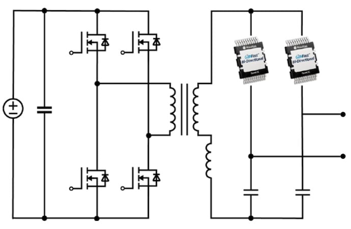
Figure 6. 500 W solar microinverter in a cyclo-converter-based topology. Image used courtesy of Bodo’s Power Systems [PDF]
Figure 7 shows a single-stage BDS that is being implemented by a leading solar microinverter manufacturer. For this, the design delivers a more powerful design (500 W) in a significantly smaller form factor, eliminating one magnetic component, and reducing the component count. This topology increases system efficiencies from 96% to 97.5% and reduces generation costs by 30%, from $0.10/W to $0.07/W.
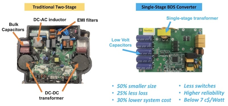
Figure 7. The 500 W solar microinverter in a cyclo-converter-based topology (circuit diagram in figure 6), with traditional 400 W 2-stage solution (left) and single-stage BDS converter solution showing reduction in size, component count, and complexity (right). Image used courtesy of Bodo’s Power Systems [PDF]
This article originally appeared in Bodo’s Power Systems [PDF] magazine.