Facebook
 Google
 GitHub
 Linkedin
Power Control at 27 MHz with Variable Reactance
This is the second of a three part series. In Part 1, we described a quasi-class E circuit providing variable power into inductive and resistive loads
This is the second of a three part series. In Part 1, we described a quasi-class E circuit providing variable power into inductive and resistive loads with a fixed supply voltage while maintaining ZIS turn-ON and ZVS turn OFF 1. In this installment, we examine reactance tuned methods providing electronically variable power.
Power output for a class E switch mode circuit may be controlled with an electronically variable reactance, by moving an L-C network up and down its resonance curve. Practically speaking, the authors are unaware of any magnetic materials that perform well as saturable reactors at 3 MHz, much less near 30 MHz. This leaves dynamic capacitance control.
The Search for a Practical Electronically-Tuned Capacitor
A diode junction has a depletion region and junction capacitance that vary with reverse voltage. This “varactor effect” has been used for electronic tuning of radio receivers, and other small signal applications for decades. Recently, an RF power amplifier technique called “load modulation” was described [2],[3]. We tested silicon fast recovery diodes, silicon carbide Schottky diodes, MOSFETs, and conventional high voltage silicon rectifiers for use as electronically tuned capacitances.
We found fast recovery diodes with suitable reverse voltage-vs.-capacitance characteristics. An RFN5TF8S is an ultra-fast rectifier with a reverse recovery time in the 30-50 nsec range. A model for this part is included with LTSpice 4. A simulation was performed with these diodes. A simulated resonant frequency range of more than 2:1 was obtained with a reverse DC bias voltage between 30 and 600 volts DC (Figures 2 and 3).
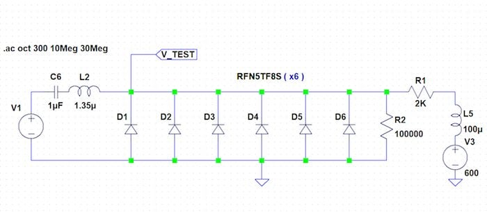
Figure 1: Diode Capacitance Simulation Circuit
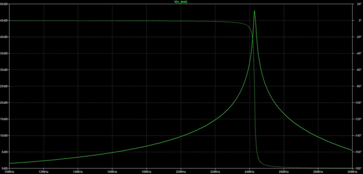
Figure 2: Simulated Response of Figure 1 with 600V Reverse Voltage
We followed with an in-circuit evaluation of these ultra-fast recovery diodes. While these simulations looked “ok”, we were surprised by in-circuit testing.
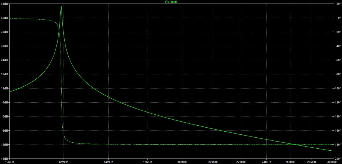
Figure 3: Simulated Response of Figure 1 with 30V Reverse Voltage
High RF dissipation was noted for the “fast” diode devices, as well as the SiC Schottky diodes. Voltage waveforms showed that neither reverse breakdown nor forward conduction was occurring. The loss mechanism was unclear.
We tried standard and super junction silicon MOSFETs as varactor diodes. To do so, we shorted the gate and source leads together, and used the drain/source terminals as a voltage-variable capacitance. Then, we placed two of these devices back to back. This resulted in another surprise, this time pleasant. A total dissipation of less than 1 watt at the 25-watt power level and less than 3 watts at the 100-watt level was noted using two SPP17N80C3 super junction devices.
Dissipation was determined by DC power substitution where DC dissipation (I x R) was adjusted to duplicate the temperature rise observed under RF conditions.
Two Cree/Wolfspeed 280 milliohm, 900-volt silicon carbide MOSFETs were tried. At 25 watts RF power, we were surprised that power dissipation was nearly 5 watts total. Calculations showed that the Miller (CGD) capacitive current multiplied by the internal gate resistance was sufficient to exceed the threshold voltage of the device, causing excess conduction loss. (See Reference 5)
Data for these parts indicated an internal gate resistance of 26 ohms. It is not clear why a technology with so much performance potential is apparently hobbled by such large internal gate resistance.
“Old-Style” Rectifier Diodes as Varactors and Switches
Standard 1N5408 3 amp 1000 volt rectifier diodes were tested as varactors with surprisingly good results. A single diode dissipated only 0.35 watts at 25 watts RF power and 2.5 watts at 100 watts RF power. Four such diodes were connected in parallel. At 100 watts RF power, the dissipation of the diode network was about 1.5 watts. Splitting C2 into C2 and C3 reduced RF voltage on the “varactor” diodes circuit in Figure 4 gives 30dB power control.
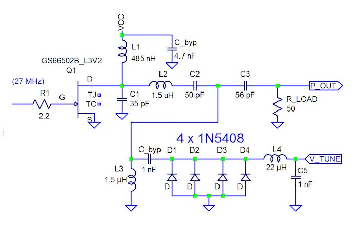
Figure 4: Varactor Power Control
A 3 bit PIN Switched Capacitor Digital Control Circuit
Next, we devised a three bit digitally switched capacitor network providing 8 capacitance steps. An ideal high-frequency capacitor switch should have near-zero resistance when “ON”, and very high resistance when “OFF”. In addition, the “off”-state capacitance should be very small. Of all the semiconductor technologies considered, only a PIN diode technique seemed feasible. Other switch technologies had too much “off” state capacitance. Specialized semiconductors are usually required at our power levels.
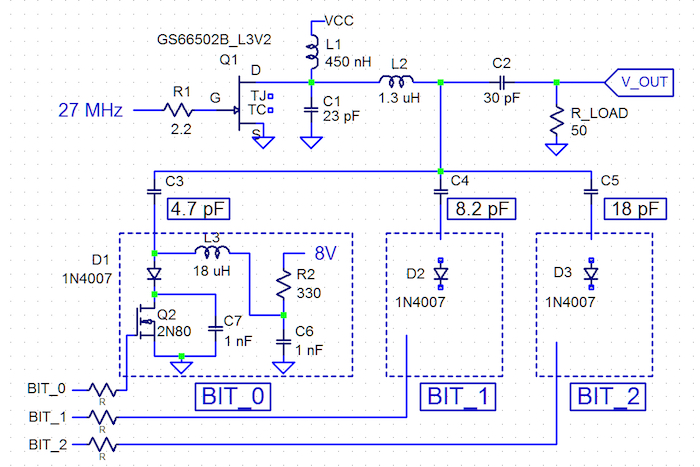
Figure 5: Power Stage with 3 Bit Tuning Network
In a nutshell, a PIN diode can control ampere-level RF currents with a DC bias current in the tens-of-milliampere range. PIN diodes have been used as RF switches from 3 MHz into the gigahertz region for several decades. In the “on” (forward-biased) state, an equivalent impedance of 0.3 – 2 ohms can be achieved. In the “off” (reverse biased) state, an equivalent series resistance of 1000 to 10,000 ohms, with a junction capacitance of 0.5 to 3 pF is attainable. A good overview of PIN diode theory and operation is available [6].
We found several RF-grade PIN diodes having suitable breakdown voltage ratings. The cost was prohibitive for these specialty parts. Standard silicon rectifier diodes with breakdown voltages above 500 volts generally have a PIN structure. Common rectifier diodes such as the 1N4007 (1A, 1000V). have been used as an inexpensive substitute for pricey RF-grade PIN diodes, controlling up to 100 watts of RF power [7].
Junction capacitance was measured for a 1N4007 rectifier. At VR of 100 volts, the capacitance was 2.6 pF. At 300V, the junction capacitance measured 1.8 pF. At 800 volts, the capacitance decreased to 1.6 pF. 1N4007 diodes from three manufacturers, having several date codes, exhibited little variation; 800 volt reverse bias capacitance ranged from 1.5 to 2.3 pF.
Figure 5 shows a schematic for our PIN switch concept. At 100 VDC input and 110 watts, maximum output the PIN switch is effectively an open circuit when reverse-biased. The inductor L3 was chosen to resonate with the PIN diode “off” capacitance, making the switch transparent to circuit operation. The temperature rise of the 1N4007 when “off” was too small to measure accurately.
In the “ON” condition, 20 ma of forwarding bias was applied to the PIN switch. The diode temperature rise was again too small to measure accurately. With 65 watts output into a 50 Ohm load, the load current was about 1.15 amperes. Since the switched capacitance is a fraction of the total tuning capacitance, the PIN switch conducts only a fraction of the total load current. If the PIN switch resistance is 1 ohm, we estimate that milliwatt level dissipation would result during the “on” state.
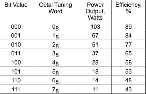
Table 1: Power Output vs. Tuning Word.
As long as no DC current is being drawn, PIN diodes tend to self-bias near the peak applied RF voltage. Thus, a high voltage negative bias source is not required to turn off the PIN diodes, simplifying the 3-bit PIN switch. The complete power amplifier and capacitor network circuit is shown in Figure 5. The power output versus tuning state, from 000 (octal “0”) to 111 (octal “7”), is shown in Table 1. Column 4 shows DC - RF efficiency for each state. The circuit connects the PIN diode to ground, simplifying drive circuitry considerably and increasing the output power range.
In the final installment, we will discuss our experiments and test results further we will look at rectification to D.C. and other issues.
References
- Pacholok, et al, “Quasi-Class E Achieves Power Control and ZIS/ ZVS”, Bodo’s Power Systems, November 2018
- S. Welton, “A Class-J Power Amplifier with Varactor Based Dynamic Load Modulation”, https://etd.ohiolink.edu/rws_etd/document/get/osu1306865537/ inline - retrieved Sept. 2018.
- W. Hallberg, “A Class-J Power Amplifier with Varactor Based Dynamic Load Modulation” http://publications.lib.chalmers.se/records/fulltext/199516/199516. pdf - retrieved Sept. 2018.
- LTSPICE simulation software: http://www.analog.com/en/design-center/design-tools-and-calculators/ltsp...
- http://www.wolfspeed.com/C3M0280090D - retrieved Sept., 2018.
- https://www.elprocus.com/pin-diode-basics-working-applications - retrieved Sept., 2018.
- http://wa5bdu.blogspot.com/2017/03/pin-diode-tr-switch.html - retrieved Sept., 2018.
About the Authors
David Pacholok has operated Creative Electronic Consultants, LLC since 1981. He is active in switchmode power conversion, electronic lighting ballasts, RF power, pulse Power, and induction heating.
Paul Reich is a freelance consultant. His specialties are radio frequency design and simulation. In a previous life, he held various positions at Motorola, Inc. and the Chamberlain Group. Paul earned his BSEE in 1976.
Jim Spangler is President of Spangler Prototype, Inc. Jim was a Field Applications Engineer at Motorola Semiconductor, OnSemiconductor, Cirrus Logic, and Active Semiconductor. Jim was involved with several IEEE societies, and planning for the PSMA Applied Power Electronics Conference (APEC). Jim has published extensively about power electronics applications.