Facebook
 Google
 GitHub
 Linkedin
Part 3 Digital Power Supply Loop Design Step-by-Step
This article highlights Biricha digital power supply loop design on how to account phase loss and scaling factors in a digital power supply.
In the previous article, we presented the linear difference equations of a 3-Pole-3-Zero (3p3z) and a 2-Pole-2-Zero (2p2z) [1] compensator but we deliberately omitted the impact of various scalings and time delays. In this article, we will show how to take these factors into account, how to mitigate their impact and therefore we will finalize the design.
The methods shown here are a subset of the material that is covered in Biricha Digital’s Power Supply Design Workshops [2]. Finally, we will verify all these design guides with a complete numerical example and provide experimental results.
How to Account for Time Delays in Digital Loop Design and Mitigate Their Impact
Pure time delays in our transfer function manifest themselves as phase loss or phase erosion. In other words, if we have some time delay in our system, such as ADC delay time, for example, we may end up with less phase margin than we expected. Therefore, we must take these into account.
Although the above may sound like a bit of a mouthful, it is very easy to visualize. Let us assume that we have a 1Hz sine wave. If we delay this sine wave by exactly 1 second, then we will have caused a phase delay of 360 degrees. If we delay it by 0.5 seconds then we will have lost 180 degrees. You can, therefore, see that there is a direct mathematical relationship between the phase loss in degrees, our frequency f, in Hz and our time delay in seconds. This is shown in the equation below [2]:
φ = 360° x ƒ x Time Delay
In our case, we are interested in our phase loss at crossover frequency fx. This is because our phase margin is defined at the crossover frequency.
So if we have a crossover frequency of 10kHz and the total time delay of 5 us (for example due to ADC sampling time) then the total phase lost at crossover i.e. total phase margin erosion would be: 360 x 10kHz x 5us = 18 degrees.
Hence, if in the analog world we wanted a phase margin of 45 degrees, all we have to do in a digital world to mitigate for this phase loss is to design our power supply with 63 degrees of phase margin. This would mean that after 18 degrees of phase loss, we will end up with a digital power supply with the desired phase margin of 45 degrees. Yes, it really is as simple as this!
Calculating the Total Pure Time Delay in a Digital Power Supply
There are two schools of thought on how much time delay there is. Some papers suggest that the total time delay in a digital power supply is simply the time taken from when you take a sample with your ADC to the time you update your PWM. This is usually 1 sampling interval for a real-time system where the switching frequency is equal to the sampling frequency.
So if you were switching/sampling at 200kHz then, each sampling interval would be 1/200kHz = 5us. Therefore, if you sampled your output voltage with the ADC on the rising edge of the PWM cycle, then you did all your calculations during this 5us and updated the new value of PWM in the next sampling interval, you would have added a pure time delay of 5us.
The second school of thought is that the total time delay is the above ADC/calculation delay PLUS ½ sampling interval due to the sampling and reconstruction. In this article, we will use this second method as it gives us a much closer match with experimental results.
Therefore our total time delay for the above 200kHz power supply with a crossover frequency of 10 kHz would be: 5us due the time we take from ADC sampling in period one and PWM updating in the next period + ½ x 5us = 2.5us due to sampling and reconstruction. This would give us a grand total time delay of 7.5 us.
From the equation above we know that total phase loss at crossover frequency would be: 360 x 10kHz x 7.5 us = 27 degrees. Let us assume once more that we would like a phase margin of 45 degrees and therefore we will design our power supply with a phase margin of 27 + 45 degrees = 72 degrees. Incidentally, this is exactly the analog power supply that we presented in the previous article before converting it into digital.
Accounting for Scaling Factors in Digital Loop Design and Mitigating Their Impact
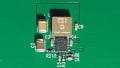
The very last thing we need to take into account is the various scaling factors. Let us assume that the output voltage of our power supply is 3.3V but we scale this down by a factor of 2 using a divide by two potential dividers before we feed it into our ADC. Let us also assume that we have a 3.3V, 12 bit ADC and therefore 3.3V on the input pin of the ADC would give us 4095 in the ADC’s Results Register. This is shown in Figure 1.
Our ADC potential divider adds a scaling factor of ½ to our system and therefore everything will be off by a factor of 0.5 unless we fix it. We can fix this very easily by “anti-scaling” everything by the reciprocal 0.5, i.e. we multiply the output of our controller y[n] by 2.
The ADC itself also adds a scaling factor. The ADC in our case (12 bit, 3.3V) takes a voltage between 0 to 3.3V and gives us a number between 0 to 4095. Therefore the gain of our ADC is 4095/3.3. In other words, everything is off by a scaling factor of 4095/3.3. Just like the potential divider in order to negate the impact of this scaling factor we have to multiply our output y[n] by 3.3/4095 also.
There is one last scaling factor to take care of and that is our PWM. Let us assume that our PWM counter counts from 0 to 20480 (i.e. period counter max value) which will give us a duty between 0 to 100%. Or, the gain of the PWM is 1/20480 and therefore to anti-scale we need to multiply the output with 20480.

Figure 1
In our case, our total “anti-scaling” factor (shown as K in the figure) is, therefore:
$$\left ( \frac{1}{0.5} \right ) \times \left ( \frac{3.3}{4095} \right ) \times (20480) = 33$$
So to get a near-perfect match with the real power supply is to multiple supplies is to multiply the output of the 3p3z linear difference equation by 33, i.e. K = 33 in the figure.
Of course the above is for a specific power supply but we can very easily make it apply to every voltage mode power supply using the following generic equation[2]:
$$\left ( \frac{1}{ADC \ Pot \ Scale \ Factor} \right ) \times \left( \frac{ADC \ Range \ in \ Volts}{(2^{ADC \ bits} -1)} \right ) \times (PWM \ Period \ in \ Ticks)$$
The principle stays exactly the same for current mode but now we also have to take in to account the DAC for the most popular implementation of digital current mode:
$$K=(\frac{1}{ADC\, Pot \, Scale Factor})\times (\frac{ADC\, Range\, in\, Volts}{(2^{ADC\, bits}-1)})\times \frac{(2^{ADC\, bits}-1)}{ADC\, Range\, in\, Volts}$$
Experimental Results and Verification of the Theory
In the previous articles we designed the control loop of our power supply to have a crossover frequency of 10kHz and a phase margin of around 75 degrees. We designed it to have 75 degrees on purpose because we know that we are going to lose 27 degrees of phase margin due to delays and after this loss, our real digital design should have around 48 degrees of phase margin.
In our previous article we placed our analog poles and zeros and calculated our coefficients to be:
B0 = (+1.212026610403)
B1 = (-1.106625987416)
B2 = (-1.209779932536)
B3 = (+1.108872665284)
A1 = (+1.590703155656)
A2 = (-0.410251039699)
A3 = (-0.180452115956)
The digital equivalent LDE for this circuit is shown below: y[n] = A1 y[n-1] + A2 y[n-2] + A3 y[n-3] + B0 x[n] + B1 x[n-1] + B2 x[n-2] + B3 x[n-3]
This equation with the above coefficients should give us around 48 degrees of phase margin but the crossover frequency will be incorrect due to scalings as mentioned before. However, we now know that if we multiply y[n] by 33 we should also get the correct crossover frequency
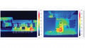
Figure 2 depicts our simulated and our experimental results for this exact power supply.

Figure 2
The green trace shows the simulated Bode plot of this power supply using Biricha Digital’s WDS Power Supply Design Software [3]. The black trace is the real measurement using an Omicron Bode-100 Vector Network Analyser.
As you can see from this Bode Plot, now that our scalings and phase delays have been taken into account we get a near-perfect match between the theoretical results and the real measurement. Our design is now complete!
In this article, we showed how to account for phase loss and scaling factors in a digital power supply. We provided exact deterministic equations to calculate the total phase loss at crossover frequency and exact equations for negating the impact of various scalings in the control loop of both voltage mode and current mode digital power supplies. We then presented experimental results showing a near-perfect match between the theory and real measurement. Our design is now complete.
As you can see there are many steps that we need to take in order to successfully stabilize a digital power supply loop and we provided these in this and previous articles.
However would it not be nice if there were a few free software packages that automated all of these? As it turns out there are and in the next article we will design a complete digital power supply from A to Z using Biricha Digital’s new completely free version of WDS digital power supply design software [3] available from ST WDS Biricha
About the Author
Ali Shirsavar holds a Doctorate of Philosophy (Ph.D.) in Power Electronics at the University of Reading, Berkshire, England. He is an Associate Professor at the University of Reading for more than 17 years then became the Director at Biricha Digital Power.
Bibliography
- Previous Biricha Lecture Notes in Bodo Power Magazine
- Biricha Digital’s “Digital PSU Design Workshop” Handbook
- Biricha Digital’s New Free Digital Power Supply Design Software
This article originally appeared in the Bodo’s Power Systems magazine.
Related Content