Facebook
 Google
 GitHub
 Linkedin
Achieving Galvanic Isolation and Protection With Solid-State Isolators—Part 2
Learn how Infineon's SSI family offers compact, efficient solid-state relays (SSRs) for high-voltage industrial systems, simplifying design over conventional SCR/TRIACs.
This article is published by EEPower as part of an exclusive digital content partnership with Bodo’s Power Systems.
Article is co-authored by Sameh Snene, Product Applications Engineer at Infineon Technologies.
An optimal isolation strategy can determine design success and accelerate time to market—especially in high-voltage industrial systems. Infineon’s SSI family offers a compact, efficient solution that integrates protection and control functions while simplifying thermal and circuit design.
This article explores practical solid-state relays (SSR) implementations using Infineon SSI and CoolMOS™ devices and compares them to conventional SSR designs based on silicon-controlled rectifiers (SCRs) or TRIACs.
The Limitations of Conventional Solid-State Relays
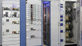
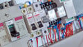
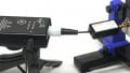
Large industrial control cabinets typically house critical power distribution components such as circuit breakers, power meters, fuses, and SSRs. As shown in Figure 1, these SSRs are commonly used to control lighting systems, ventilation groups, air conditioners, refrigeration lines, and other infrastructure loads.
Figure 1. DIN rail mount SSR (A, B and C) and a DIN rail Fuse socket (D). Image used courtesy of Bodo’s Power Systems [PDF]
Compared to electromechanical relays (EMRs), SSRs deliver longer operating life and enable remote capabilities. However, SSRs based on TRIACs or SCRs are often challenged by high power dissipation, large heat sink and board space requirements, and a lack of integrated fault protection. Additional challenges include limited DC operation due to forced commutation techniques and an absence of real-time fault monitoring.
The limitations of conventional SSRs in real-world products are highlighted by evaluating a typical DIN rail-mounted SSR. This 6A, single-phase relay uses a random-voltage switching SCR output. It accepts 4–32 V DC input and supports 24–280 V AC output at up to 6 A. At full load, the voltage drop is <1.3 V, resulting in ~7.8 W power dissipation.
The SSR lacks integrated protections. Off-state leakage is 0.1 mA, while turn-on and turn-off times are 0.1 ms and 0.5 cycles, respectively. dv/dt immunity is 500 V/μs and fusing thresholds are 410 A²·s (50 Hz) and 375 A²·s (60 Hz). Load current ranges from 150 mA to 6 A.
Without built-in protection, a large portion of the housing is dedicated to heat sinking. In space-constrained DIN-rail cabinets with poor airflow, heat buildup can shorten service life.
The Advantages of SSI-Based SSRs
SSI devices provide compelling benefits in power distribution environments, particularly in applications where SSRs based on TRIACs or SCRs are used. Importantly, an optimal isolation strategy directly determines design success and time-to-market.
Solutions with integrated features that support high-voltage circuitry across a broad range of industrial and commercial applications offer definitive advantages, particularly when addressing diverse system requirements.
Here, we compare the DIN rail SSR with a solution built around Infineon’s SSI technology. Because this is an AC application, two CoolMOS™ devices are required. Our goal is to reduce on-state power dissipation by a factor of three at full output current. To meet this target, the required total Rds(on) can be estimated using:
\[Rds_{on}=\frac{Pdiss}{3*2*Imax^{2}}=\frac{7.8}{3*2*6^{2}}=36m\Omega\]
Where Pdiss is the reference SSR’s power dissipation (7.8 W), and Imax is the maximum output current (6 A). This implies that each MOSFET should have an Rds(on) below 36 mΩ.
Based on the CoolMOS™ options available, the IPT60T022S7 in a TO-LEADLESS (TOOL) package meets this requirement, with an Rds(on) of 22 mΩ at 25°C. While Rds(on) will approximately double at 150°C, the device still stays within target limits.
For better thermal protection and real-time temperature monitoring, a T-series CoolMOS™ device with an integrated temperature sensor is recommended. This enables accurate die temperature tracking and minimizes the risk of SSR failure due to thermal overload. For this reason, the selected gate driver for this example is the iSSI30R12H, which features independent thermal and current sense input pins.
Next, we calculate the minimum buffer capacitance (Cbuf_min) required at the BUF terminal using the following equation:
\[Cbuf\_min=1.2*\frac{Qm1+Qm2}{Vbuf_{th\_min}-V_{g\_min}}\]
Where:
• Qm1 and Qm2 are the gate charges of the MOSFETs at the desired turn-on gate voltage (Vg_min)
• Vbuf_th(min) is the minimum fast turn-on comparator threshold voltage from the iSSI30R12H datasheet
• Vg_min is the minimum gate-source voltage required to fully turn on the MOSFETs
• The 1.2 factor adds margin for gate charge tolerance
In AC operation, the MOSFETs alternate between conducting and blocking. When one device is in conduction via its body diode, it functions like a synchronous rectifier. In this condition, the gate charge during turn-on bypasses the Miller plateau, resulting in a lower effective Qm. As such, Qm1 and Qm2 are different and must be derived from the gate charge curves in the datasheet.
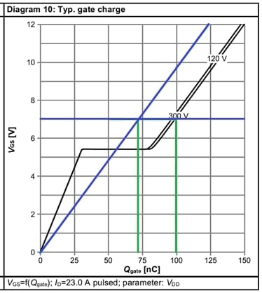
Figure 2. Extrapolation of Qm1 and Qm2 from the gate charge characteristic. Image used courtesy of Bodo’s Power Systems [PDF]
For the example design using the iSSI30R12H driver and IPT60T022S7 MOSFETs:
• Qm1 = 100 nC (CoolMOS™ off/open)
• Qm2 = 70 nC (CoolMOS™ conducting via body diode)
• Vbuf_th(min) = 10 V (datasheet)
• Vg_min = 7 V (MOSFET gate threshold for reliable turn-on)
Substituting the formula:
\[Cbuf=1.2*\frac{100nC+70nC}{10V-7V}=68nF\]
Leakage Current in Off-State
When the SSR is off, leakage current flows through the MOSFETs due to the absence of an air gap. This leakage stems from two primary sources: Zero gate voltage drain current (IDSS) and output capacitance energy-related (Co(er)).
For the IPT60T022S7, the datasheet values are:
• IDSS = 50 µA (typ) @ VDS = 600 V, VGS = 0 V, Tj = 150°C
• Co(er) = 303 pF @ VDS = 0–300 V
When off, one MOSFET conducts through its body diode during each AC half-cycle, while the other sees the full 0–320 V swing.
The resulting current through Co(er) for a 50 Hz AC line is:
I_Co(er) = 320 / [1 / (2π × 50 × 303 pF)] ≈ 30.5 µA
Adding both effects gives the worst-case leakage current at 150°C of:
I_leak ≈ 50 µA + 30.5 µA = 80.5 µA
Protections: Short Circuit
Using MOSFETs instead of SCRs enables fast short-circuit protection. Traditional SSRs require fuses—slow to react, bulky, and single-use. A short on one load can also trip the breaker and shut down multiple lines.
In contrast, Infineon’s SSI with CoolMOS™ enables precise, real-time intervention. The CS pin on the iSSI30R12H has a 200 mV threshold. To trigger protection at ~10× the rated current (6 A), the shunt resistor is calculated as:
R_shunt = 200 mV / (10 × √2 × 6 A) ≈ 2.4 mΩ
The total SSR resistance at 150°C, including two IPT60T022S7 devices and the shunt, is:
R_total ≈ 2 × 2 × 22 mΩ + 2.4 mΩ ≈ 90.4 mΩ
V_drop = 90.4 mΩ × 6 A ≈ 542 mV
This is ~58% lower than the 1.3 V drop of the SCR-based SSR, enabling smaller heat sinks.
To avoid noise-triggered faults, a low-pass filter is added at the CS input, resulting in:
R_f = 100 Ω, C_f = 1 nF
f_p = 1 / (2πRC) ≈ 1.59 MHz
The protection response time is:
T_OC = t_CS(off) + Q_g / I_off ≈ 1 µs + 150 nC / 488 mA ≈ 1.48 µs
Overtemperature Protection
The iSSI30R12H integrates thermal protection by sourcing a 50 µA bias current to monitor the CoolMOS™ die temperature. Shutdown is triggered when the sensor voltage drops below 1.095 V, corresponding to a junction temperature of ~155°C.
The device includes a built-in comparator with noise filtering. To further stabilize readings, an external RC filter matching the overcurrent filter frequency is recommended:
R_f = 100 Ω, C_f = 1 nF → f_p ≈ 1.59 MHz
This configuration ensures fast, reliable thermal shutdown and helps protect the MOSFETs under high-load conditions.
Transient Voltage Suppression and Miller Clamping Protection
To protect the MOSFETs from voltage spikes during fault conditions or inductive load switching, a TVS or MOV (shown as D1 in Figure 3) should be mounted close to the MOSFET drains. The clamp’s breakdown voltage must exceed the SSR’s peak line voltage but remain below the CoolMOS™ breakdown threshold.
For 280 V AC operation:
V_peak = 280 V_AC × √2 ≈ 396 V
An ideal TVS option is SMCJ400CA, with a 400 V standoff and 1,500 W peak power rating.
Surge transients can also induce high dv/dt across switches, which may couple through parasitic capacitances and cause unwanted turn-on. The iSSI30R12H includes a Miller clamp to prevent this.
Datasheet values:
• V_MC max = 3.6 V, R_MC = 600 Ω
• Assume dv/dt = 10 V/ns
I_MC = 3.6 V / 600 Ω = 6 mA
C_MC(min) = 6 mA / (10 V/ns) = 0.6 pF → use 1 pF
Optionally, a 3.3 V Zener can be added between each MC pin and GND2. However, this is often unnecessary since the device tolerates up to 100 mA for sub-1 µs pulses.
Input Stage
The iSSI30R12H supports separate Vcc1 and IN pins, allowing multiple devices to be driven in parallel from a 3.3 V microcontroller. For single wide-range input, Vcc1 and IN can be tied together, requiring only one input resistor— that must be sized for the clamped Vcc1 max of 3.5 V.
For 12–24 V industrial inputs:
R_in = (12 V − 3.5 V) / 16 mA ≈ 536 Ω (E48)
Input power at 24 V:
P_in = (24 V − 3.5 V) / 536 Ω × 3.5 V ≈ 134 mW
Resistor power dissipation:
P_R = (24 V − 3.5 V)² / 536 Ω ≈ 784 mW
Use a 1–1.5 W resistor, or a 3.3 V DC/DC converter for better efficiency. The bypass capacitor can be sized from datasheet specs:
C_in = 3.3 nF (max 4.7 nF)
Component Summary: DIN Rail SSR
With all key components selected, the SSR output stage is defined as shown in the schematic. Using iSSI30R12H and 2× IPT60T022S7, we compare the new design against the commercial reference. Table 2 summarizes performance across metrics such as Rds(on), power dissipation, protection response, and thermal behavior. This comparison highlights improvements in efficiency, protection, and footprint enabled by Infineon’s SSI-based SSR architecture.
| Schematic reference | Calculation reference | Value | Comments |
| U1 | U1 | iSSI30R12H | Infineon SSI |
| T1, T2 | PT60T022S7 | IPT60T022S7 | Infineon CoolMOSTM T-series |
| Rsh | Rsh | 2.4m | Shunt resistor |
| D1 | TVS | SMCJ400CA | 1500W in SMC package |
| D2, D3 | DZ | 3.3V | Diode zener 500mW |
| R3, R4 | Rfoc, Rfot | 100Ω | smd resistor |
| R5, R6 | none | 0 Ω | Not used |
| C3, C4 | CMC | 1pF | 2kV smd capacitor |
| C5 | Cbuf | 68nF | 50V smd capacitor |
| C6, C7 | Cfoc, Cfot | 1nF | 50V smd capacitor |
| R1 | Rin | 536Ω | 1W resistor |
| C1 | Cin | 3.3nF | 25V smd capacitor |

Figure 3. SSR application schematic. Image used courtesy of Bodo’s Power Systems [PDF]
Table 2. DIN rail SSR solution comparison
| Specification | Single phase SSR, 6A, DIN rail | Single phase SSR, 6A, DIN rail (iSSI30R12H + 2x IPT60T022S7) |
| Type | Random voltage switching SCR Output | Random voltage switching MOSFETs Output |
| Operating Voltage / Current | 4 - 32 VDC Input 24 - 280Vac Output, 6 A | 12-24 VDC Input 24 - 280Vac Output, 6 A |
| Maximum Voltage Drop | < 1.3V (on – state) Pdissmax = 1.3*6A = 7.8 W | < 542 mV (on – state) Pdissmax = 0.542*6 A = 3.25 W |
| Maximum T for Fusing | 410 A².s for 10 ms at 50 Hz * 375 A².s for 8.33 ms at 60 Hz * * No protections | Over Current protection set at 60 Arms (≅ 85A peak) Over Temperature Protection set at Mosfets’ Tj = 155°C |
| Maximum Leakage Current | 0.1 mA (off state) | < 36 uA @ Tj=25°C |
| Load current | 0.15 – 6 A | 0 – 6 A (no minimum holding) |
| dV/dt | 500 V/µs off-state at maximum voltage | > 10 V/ns, with protection |
| Response Time | 0.5 cycle (turn-off) 0.1 ms (turn-on) | ~2.5 ms (turn – on) < 1.5 µs (turn-off in OCP & OTP) |
Table 3. Commercial panel mount SSR characteristics
| Specification | Pre-Assembled ‘Hockey Puck’ |
| Type | Single Phase Panel Mount SCR Output / Zero Voltage Switching |
| Operating Voltage / Current | 3-32 VDC input 24 - 280Vac Output, 25 A |
| Maximum Voltage Drop (Power Dissipation) | < 1.35V on-state = 1.35*25 = 33.75 W |
| Maximum T for Fusing |
370 for 8.33 ms @ 60 Hz* 380 for 10 ms @ 50 Hz* *No protections |
| Maximum Leakage Current | 0.1 mA Off state |
| Load current | 0.05 – 25 A |
| dV/dt | 500 V/us off-state |
| Response Time |
0.5 cycle (turn-off) 0.5 cycle (turn-on) |
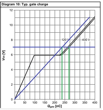
Figure 4. Rds(on) and Qg values for IPDQ 60R007CM8. Image used courtesy of Bodo’s Power Systems [PDF]
Panel-Mount SSR Overview
The panel-mount SSR example follows the same design approach, targeting a 25 A output. Based on thermal and Rds(on) targets, IPDQ60R007CM8 is selected for its low 7 mΩ resistance at 25°C. At an average operating temperature of 85°C, its Rds(on) rises to ~10.15 mΩ, which remains acceptable without paralleling devices. For optimal thermal performance, two IPDQ60T010S7 devices can be used in parallel, though at a slightly higher cost.
Since the selected CoolMOS™ doesn’t feature integrated temperature sensing, the design uses the iSSI30R11H paired with an external PTC—B59721A0100A062—for thermal protection. Based on its 200 mV threshold and internal 50 µA bias current, shutdown occurs around 92–100°C at the heat sink.
Thermal Optimization and Temperature Protection
In this example, the B59721A0100A062 PTC is used, with its resistance-temperature curve shown in Figure 5. The iSSI30R11H triggers thermal protection when its VTS input goes above 200 mV. With a typical internal current source of 50 µA, this corresponds to:
R_OTP(typ) = 200 mV / 50 µA = 4 kΩ
This equates to a heatsink temperature between 92°C and 100°C. For accurate operation, tolerances in the internal current source and comparator threshold must be factored into the design.
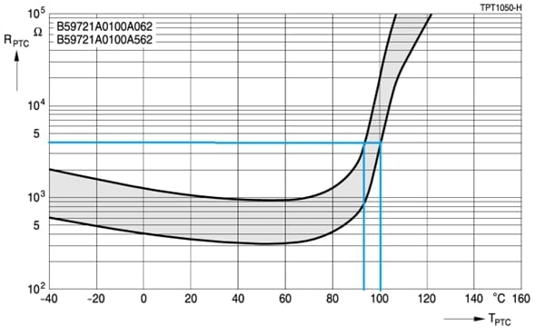
Figure 5. B59721A0080A062 PTC characteristic. Image used courtesy of Bodo’s Power Systems [PDF]
Component Summary: Panel-Mount SSR
With all components selected, calculated as for the previous paragraph, we can complete the DIN rail SSR design as shown in the schematic below.
Table 4. Component summary for a 600V - 25A SSR
| Schematic reference | Calculation reference | Value | Comments |
| U1 | U1 | iSSI30R11H | Infineon SSI |
| T1, T2 | IPDQ60R007CM8 | IPDQ60R007CM8 | Infineon CoolMOSTM 8 R-series |
| Rsh | Rsh | 590 m | Shunt resistor |
| D1 | TVS | SMCJ400CA | 1500W in SMC package |
| D2, D3 | DZ | 3.3V | Diode zener 500mW |
| R3, R4 | Rfoc, Rfot | 100Ω | smd resistor |
| R5, R6 | none | 0 Ω | Not used |
| C3, C4 | CMC | 1pF | 2kV smd capacitor |
| C5 | Cbuf | 220nF | 50V smd capacitor |
| C6, C7 | Cfoc, Cfot | 1nF | 50V smd capacitor |
| R1 | Rin | 536Ω | 1W resistor |
| C1 | Cin | 3.3nF | 25V smd capacitor |
| PTC | ROTPtyp | B59721A0100A062 | Temperature sensor |
Using the kit parts—iSSI30R11H and 2× IPDQ60R007CM8 — we compare performance against the original commercial SSR. The comparison includes key metrics such as on-state voltage drop, thermal behavior, switching response, and protection features. Results are summarized in the following table.
Table 5. Panel mount SSR solution comparison
| Specification | Pre-Assembled ‘Hockey Puck’ | Single phase SSR, 25A, DIN rail (iSSI30R11H + 2x IPDQ60R007CM8) |
| Type | Single Phase Panel Mount SCR Output / Zero Voltage Switching | Single Phase Panel Mount Random voltage switching MOSFETs Output |
| Operating Voltage / Current | 3-32 VDC input 24 - 280Vac Output, 25 A | 12-24 VDC Input 24 - 280Vac Output, 25 A |
| Maximum Voltage Drop | < 1.35V on-state Pdissmax =1.35*25 = 33.75 W | < 522mV (on – state @ Tj=85°C) Pdissmax = 0.522*25A = 13.05 W |
| Maximum T for Fusing | 370 for 8.33 ms @ 60 Hz* 380 for 10 ms @ 50 Hz* *No protections | Over Current protection set at 250 Arms (≅ 350 A peak), Over Temperature Protection set at Tc = 92°C to 100°C |
| Maximum Leakage Current | 0.1mA Off state | < 66 μA @ Tj=25°C |
| Load current | 0.05 – 25A | 0 – 25 A (no minimum holding) |
| dV/dt | 500 V/µs off-state at maximum voltage | > 10 V/ns, with protection |
| Response Time | 0.5 cycle (turn-off) 0.1 ms (turn-on) | < 2.0 µs (turn-off in OCP & OTP) ~8 ms (turn – on) |
Conclusion
Infineon’s new family of SSIs simplifies SSR development for industrial and commercial applications. Optimized for use with CoolMOS™ devices, these isolators establish a new performance benchmark in SSR design.
Together, the SSI and CoolMOS solution deliver key advantages over traditional TRIAC- or SCR-based SSRs—including up to 50% lower power dissipation, smaller heat sinks, reduced board space, and lower system weight. Integrated overcurrent and overtemperature protection eliminates the need for external fuses.
The MOSFET-based output stage enables fast switching, DC operation, and removes minimum load constraints. Leakage current is reduced, and dv/dt immunity exceeds 1,000× that of conventional designs.
These improvements enable short-circuit-protected SSRs that reduce thermal stress, save space, and improve reliability in power distribution systems. By streamlining protection, control, and thermal design, Infineon’s SSIs help reduce development cycles, ensure design success, and accelerate time to market.
This article originally appeared in Bodo’s Power Systems [PDF] magazine and is co-authored by Davide Giacomini, Director of Marketing, Power IC Group, and Sameh Snene, Product Applications Engineer, both Infineon Technologies