Facebook
 Google
 GitHub
 Linkedin
Dynamic Characterization of GaN Power Semiconductor Devices
This article highlights Keysight Technologies that overcome the challenges associated with GaN FET dynamic characterization.
As we’ve discussed in our last few articles, dynamic characterization of Silicon Carbide (SiC) power semiconductor devices poses a lot of design challenges to make repeatable and reliable double pulse test solutions. Gallium Nitride (GaN) power semiconductor field-effect transistors (FET) present even more difficult challenges because of its higher frequency operation and multiple variations of technology. In this article, we discuss how we overcome the challenges associated with GaN FET dynamic characterization.
Challenges for GaN FET dynamic testing There are a few variations in GaN FETs. Typical types are listed below.
- GaN HEMT (Hi Electron Mobility Transistor)
- Gate Injection Transistor (GIT)
- Cascode GaN FET

Figure 1: GaN FET double pulse test results with oscillation. Figure 2: Distorted current measurement results on GaN FET.
They have different structures, behaviors, and properties. Therefore, each type requires different gate driving control, but all of them operate faster than their silicon or silicon carbide (SiC) counterparts, with typical transition times less than 10ns. Such an extremely fast speed brings about a lot of challenges for testing. Fast dv/dt and di/dt triggers ringing or oscillation and deteriorates measurement accuracy. Such oscillation sometimes destroys DUTs (Device Under Test) as shown in Figure 1.

Figure 2: Distorted current measurement results on GaN FET.
Fast di/dt makes current measurement very difficult, because there is no commercially available current sensor which has both high bandwidth and low insertion inductance. Current sensors such as the Rogowski coil have less than 50MHz bandwidth, which is not enough for capturing current transitions less than 10ns. The Pearson probe can have up to 200MHz bandwidth, but its large size increases the test power loop inductance and therefore, deteriorates the measured waveform. Commercial coaxial shunt resistors have higher bandwidths, but their large insertion inductance causes ringing and voltage distortion (Figure 2). Because the parasitic inductance in the test circuit causes various issues such as ringing, it is common sense to solder the DUT to the test board to minimize the parasitic inductance. Unfortunately, it is very inconvenient if you need statistical results using multiple devices, because soldering/unsoldering devices quickly wears out the test board. Fixtures exist with spring type connectors, which allow solderless contact for SMD type devices. However, even such a tailor-made fixture has non-negligible parasitic inductance.
It would be ideal to have a one-size-fits-all test system for all GaN FETs. This goal is impractical for multiple reasons. Fast operating speeds of GaN FETs require the package of the device to be small to maximize the performance. However, there is little package standardization across the various GaN FET types. In addition, the different GaN FET types require different gate driver, components, layouts, and even different topology designs. Therefore, a test board must be made for each DUT, matching PCB contacts with the pad pattern of each DUT. Fortunately, most of the Double Pulse Test (DPT) system can remain standard.
Technologies to solve the challenges As we’ve discussed in previous articles, the best method to minimize the test circuit parasitics is to reduce the test circuit area. Having smaller power loops and gate loops effectively reduces the associated parasitic inductance and therefore, reduces measurement waveform distortion such as ringing. In practice, reducing the power loop is not simple, because you must provide a method to measure current and voltage in this loop, as well as mechanism to connect the DUT.
Current measurement is a big problem as already shown in Figure 2. To solve this challenge, we developed a current sensor. Although a thorough analysis of the sensor’s performance is still ongoing, double pulse test results indicate a much lower insertion inductance and superior bandwidth compared to other commercially available solutions.
As mentioned previously, soldering the DUT to minimize parasitic inductance is cumbersome and inefficient for double pulse test systems. A solderless contact with minimal parasitics is attainable. We’ve developed a solderless contact, minimizing contact inductance between the DUT and the PCB and achieved accurate mechanical aligning with a customizable DUT holder. (Figure 3). The parasitic inductance is much less than a typical DUT fixture with spring type connectors. The combination of designing a small circuit loop area, using a high bandwidth/low inductance current sensor, and attaching the DUT via a low inductance, solderless connection can provide you with very clean measurement waveforms. Clean waveforms allow more repeatable and reliable extractions of the desired switching parameters.

Figure 3: Newly developed solderless DUT interface.
In the last few articles, we discussed what we call the AUTOCAL function which calibrates various errors for voltage and current measurements and for timing misalignment. The same philosophy and technology can be applied for the GaN FET testing if the test board is designed right, enabling repeatable and reliable dynamic measurements even for GaN FETs.
For GaN FETs, dynamic Ron is a critical parameter to characterize the dynamic performance. So much in fact, that the JEDEC JC70.1 task group chose this parameter as their first defined test method, using a clamp circuit for Vds measurements. [1] The idea is to clamp the voltage to a much lower value (e.g. 5V) than applied Vds voltage (e.g. 400V). This allows the use of another channel of the oscilloscope to monitor the Vds voltage with much higher resolution (i.e. a standard low voltage probe can be used).
In summary, various advanced techniques/technologies shown beloware necessary to make accurate dynamic characterization of GaN FET.
- Small size test circuit
- Low insertion inductance current sensor
- Non-solder contact technology
- AUTOCAL implementation for repeatable/reliable measurements
- Dynamic Ron measurement using clamp circuit
Keysight’s solution for GaN power FET dynamic testing Definition and development of a commercial double pulse test system for GaN FETs was a big challenge for Keysight. Not only the development of previously mentioned technologies, but also our approach to provide each customer with a tailored advanced solution, while keeping the modularity, comprehensiveness, and ease-of-use of our PD1500A Dynamic Power Device Analyzer/Double Pulse Tester.
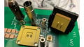
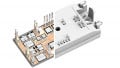
Because the test board must be fabricated for each DUT type, our strategy is to have a tailored, add-on type board for the PD1500A as illustrated in Figure 4. Each tailored GaN test board has an EEPROM which stores unique DUT information such as maximum Vgs, Vds, Id, and clamp circuit voltage. This allows seamless integration of the GaN test board onto the PD1500A, so the software can use those values to avoid potentially dangerous test conditions and the user can perform tests safely and intuitively. Figure 5 shows an example of a tailored board for a GaN eHEMT device.

Figure 4: Tailored GaN test board for PD1500A.

Figure 5: GaN tailored test board for eHEMT.
So how do these technologies impact the DPT waveforms of real GaN FETs? Figure 6 and 7 show measurement results for GIT and eHEMT. All the results show less than 5ns transition times (tr and tf) though relatively large gate resistance was used for GIT for this evaluation. Even for these fast transition times, the waveforms are clean with minimal amounts of ringing, allowing for repeatable and reliable switching parameter extractions.

Figure 6: Test results (turn-on & turn-off) for GIT (DUT: PGA26E19BA (Panasonic)).

Figure 7: Test results (turn-on & turn-off) for eHEMT (GS66508B (GaN Systems)).
Figure 8 shows measurement results of dynamic Ron for GIT. The difference in resolutions between the clamped and unclamped Vds waveforms (10X) significantly improves the resolution and accuracy of the Ron measurement.
The newly developed solderless DUT connection technology also allows for temperature measurement and control. This feature provides the capability for important temperature dependent measurement as shown in Figure 9.

Figure 8: Dynamic Ron for GIT.

Figure 9: Temperature dependent measurement for GIT.
As mentioned previously, updated PD1500A software will automatically detect the GaN tailored test boards. Standard PD1500A software features such as waveform capture, switching parameter extraction, switching locus drawing, data saving, etc. are available (Figure 10).
Because GaN FETs have many variations, Keysight has a vision and strategy to accumulate knowledge and expertise in the format of schematic, board layout, and bill of materials (BOM). Our goal is to provide tailored solutions for each customer.

Figure 10: PD1500A user interface for GaN test.
Summary
GaN FET dynamic characterization is the most challenging of the newer power semiconductor devices. Using our measurement science experience and some key investments in industry leading technology, Keysight developed these technologies to enable repeatable, reliable, and accurate dynamic characterization of GaN FETs. The PD1500A Dynamic Power Device Analyzer/Double Pulse Tester now accepts tailor-made add-on GaN FET test boards to allow dynamic characterization of Si, IGBT, SiC and GaN power devices on a single test platform.
References
Dynamic ON-Resistance Test Method Guidelines for GaN HEMT based Power Conversion Devices, Version 1.0, JEP173.
About the Author
Ryo Takeda works as a Solution Architect at Keysight Technologies Incorporated, a company driven to deliver breakthrough solutions and trusted insight in electronic design, test, manufacture, and optimization to help customers accelerate the innovations that connect and secure the world.
Bernhard Holzinger works as a Technical Architect at Keysight Technologies Incorporated, a company driven to deliver breakthrough solutions and trusted insight in electronic design, test, manufacture, and optimization to help customers accelerate the innovations that connect and secure the world.
Michael Zimmermann is an R&D Engineer at Keysight Technologies Deutschland GmbH.
Mike Hawes is the automotive and energy solutions planning manager at Keysight Technologies. Hawes holds a Master's Degree in Biomedical Engineering from Colorado State University. He also holds a Bachelor's Degree in Electrical Engineering from Washington State University.