Facebook
 Google
 GitHub
 Linkedin
New Contender for the Power Transistor Throne
This article highlights Panasonic Hybrid Drain Gate Injection Transistor (HD-GiT) with overview of advantages that aimed aimed at power converters.
How GaN is threatening the MOSFET’s crown
For more than 35 years, power MOSFETs have dominated the field of power converter design in the low to medium power range. This has been supported by continuous innovation in the components structure and related semiconductor technology. Fast switching characteristics and low losses, as well as ease of use in various circuit topologies also contributed to their success.
Silicon MOSFET technology
At the dawn of a new millennium, however, silicon power MOSFETs are reaching their theoretical performance limits, which means that further progress in power supplies and power management systems will no longer be as easy to achieve with these switching elements.
The characteristics of GaN
The first GaN power transistors were introduced in the early 2000s, after being used over a decade as a standard fixture in high-frequency technology. The favourable combination of chemical-physical characteristics offered by GaN - such as ten times the dielectric strength of silicon, high electron mobility and carrier density, very fast carrier recombinations, and last but not least a high maximum junction temperature of over 400°C –open up additional prospects for this material.
Applied to power transistors, these characteristics enable the manufacturing of high-switching frequency capable transistors. These in turn improve the power density of power conversion systems, thanks to lower conduction losses, and thanks to a reduction of the typical system size and weight – for example by reducing the size of passive components under fast switching conditions.
Gallium Nitride transistors are therefore becoming a realistic and attractive alternative to silicon transistors and start conquering the field of power electronics.
Overview and advantages of the Hybrid Drain Gate Injection Transistor (HD-GiT) structure from Panasonic
Many GaN switches in the 600 V range presented up to now had the disadvantage of being self-conducting (normally ON). Unlike MOSFETs, this means that they conduct current when no gate voltage is applied. As a countermeasure, some manufacturers have implemented cascode structures to obtain normally OFF switches. Cascode structures have major drawbacks as compared with single normally off transistors though, such as the impossibility to directly control the switching speed of the GaN element, the increased manufacturing complexity, and increased parasitic elements due to the nature of the circuit.
Panasonic X-GaNTM transistors in contrast are a normally-OFF enhancement of the High Electron Mobility Transistor structure (HEMT). Like in HEMTs a very mobile 2D electron gas is generated at the boundary between two materials with different band gaps. An added p-doped gate structure gives to the X-GaN transistors their normally off characteristic (see Figure 1). The proposed transistor structure is called Hybrid-Drain Gate Injection Transistor (HD-GiT).
Figure 1: Hybrid-Drain Gate Injection Transistor (HD-GiT)
Since the HD-GiT gate can be accessed directly, the gate circuit can be design to control and adjust the transistor’s du/dt and di/dt – a major advantage as compared with the cascade.
The lateral structure of the GiT is also advantageous for fast switching, since its parasitic capacitances are typically lower than those of vertical structures, such as for example silicon-based super-junction MOSFETs (see Figure 2).
The Figure-of-Merit (RDS(on) ∙ QG) of a 600V/70nOhm GiT is therefore ~350 mΩ ∙ nC, in other words around one tenth the value of modern silicon components.
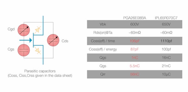
Figure 2: Parasitic capacitances are typically lower
Gate driving principle
The GiT transistor is controlled as mix of a field effect transistor and (bi)polar transistor. As with FETs, a positive threshold voltage needs to be applied between the source and gate to open a conductive channel. At the same time, a small ON-time current needs to flow into the gate to increase the conductivity of the conductive layer and to keep the switch-ON resistance as low as possible in the useful operating area.
The transistor is switched OFF by removing the voltage from the gate; the gate current stops, the channel closes, the transistor is blocking again. Unlike with IGBTs however, the charge recombinations at switch OFF do not result in measurable delays or power losses due to tail currents (see Figure 3).

Figure 3: Charge recombinations at switch off do not result in measurable delays or power losses due to tail currents
X-GaN™ GiT transistors allow current to flow in the reverse direction once the source, gate, and drain potential are set in a way that current is fed in at the gate. Unlike with MOSFETs the reverse current does not flow through a parasitic body here, instead is it conducted through the channel. Even though they are reminiscent of a diode, the thresholds in the third quadrant of the static IV curve are not dictated by junction’s behaviour, but are simply the threshold voltage of the transistor plus any negative bias voltage that is applied to the gate.
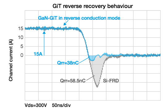
Figure 4: Conduction and recovery performances of the GiT in the reverse mode are the same as those of an SiC Schottky diode
In the same way as a MOSFET, the GiT can be switched ON in the reverse direction in order to further reduce the losses by operating under 0V-offset condition. The GiT recovers extremely quickly from reverse conduction. The recovery energy practically just corresponds to the energy required to charge the output capacitance. The conduction and recovery performances of the GiT in the reverse mode are the same as those of an SiC Schottky diode (see Figure 4).
Panasonic’s HD-GiT structure eliminates the problem of current collapse
Developers of gallium nitrite components have to deal with the phenomenon of current collapse., When the transistor is under high voltage stress, conduction electrons can become trapped in defects in the crystal, at interfaces between layers etc., which can leads to a rapid increase of the RDS(on) (on-resistance), leading to a rapid increase in losses and the destruction of the components. This effect can be especially critical for hard switched topologies.
So far Panasonic has been the only provider of GaN components to publicly announce the complete elimination of the problem of current collapse. The figure 5 shows Panasonic’s unique approach for solving the issue. An additional p-doped structure, similar to the gate, is grown near the drain and electrically connected to it. That structure injects holes into the GaN components, that recombine with the trapped electrons.
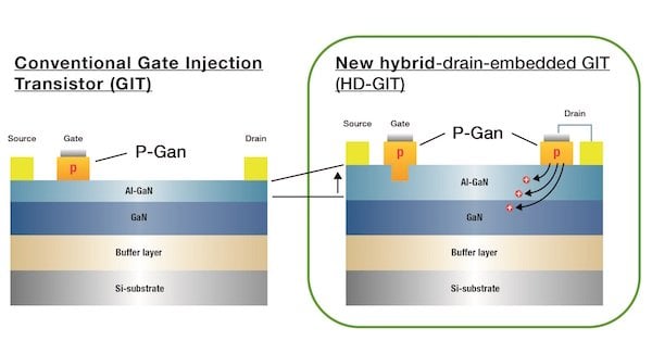
Figure 5: An additional p-doped structure, similar to the gate, is grown near the drain
The HD-GiT uses a recessed gate so that the thickness of the AIGaN layer is increased in order to avoid depletion of the charge carriers under the p-doped area close to the drain. The HD-GiT was proven to have the same excellent switching characteristics as the conventional GiT structure.

Figure 6: Using available high-performance MOSFET gate drivers
Reliability
In order to guarantee the reliability of the HD-GiT transistors in mass production, Panasonic not only tests against the usual JEDEC standards for Si components, but also developed its own additional GaNspecific tests to guarantee the long-term stability of the transistors, for example with regard to current collapse. Accelerated life tests have showed a worst case FiT rate of ~10 FIT can already be achieved.
Applications of GiT transistors Gate driving In addition to selecting the right topology and gate control scheme, the choice of the gate driver circuit is especially important. Fortunately, a simple and common push-pull gate triggering circuit with separate switch-on and switch-off resistors can be used. Figure 6 shows a typical gate circuit for GiTs that can be realised using available high-performance MOSFET gate drivers.
The designer can easily control the switching behaviour of the transistor, as shown on Figure 7 (example of dv/dt control at turn ON).
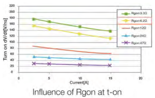
Figure 7: Control the switching behaviour of the transistor
As well as providing the necessary dynamic power during the switching transition, the gate driver must also reliably keep the transistor turned ON. The gate input characteristic of the GaN GiT corresponds to a diode (see Figure 2). The constant gate current flow through this internal gate diode Dgs during the ON-time is controlled by Rig during the on interval (Figure 5).
Finally, keeping the transistor reliably switched off requires attention, because the threshold voltage of GiTs is significantly lower than the typical level in MOSFETs. Even though the small Crss/Ciss ratio of the X-GaN transistors protects against Miller capacitance coupling effects, a negative voltage can be optionally applied to the gate during the off time to increase the safety margin.
Panasonic gate driver IC
Panasonic brought out its own X-GaN™ gate driver at the end of 2016 for developers who want to quickly deploy a solution using GiTs. The X-GaN driver IC is optimized for high switching frequencies up to 2 MHz and provides an easy way to unlock the full performance of the transistors. Besides optimized gate control terminals, additional integrated functions are provided - such as a charge pump for (optionally) generating negative gate voltages, or safety features against under-voltage and gate oscillations (Figure 8).
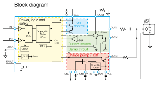
Figure 8: X-GaN driver IC is optimized for high switching frequencies
Advantages in applications
Panasonic’s GiT transistors are aimed at power converters in the ~100 W to ~5-6 kW range, where MOSFETs with 600 V to 650 V are typically used today. Depending on the requirements of the application, developers can target maximum efficiency, maximum power density, or a compromise between the two.
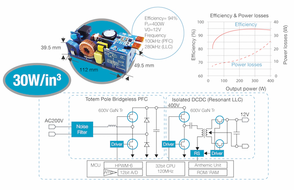
Figure 9: Compact and efficient AC-DC demo unit
Thanks to their “0 reverse recovery” behaviour, GaN transistors make some topologies practically usable, such as for example totem-pole PFCs, which require fewer parts as conventional designs and exhibit state-of-the-art efficiency performance.
Increased switching frequency enables passive components to be miniaturized – in particular magnetic components – whereas the power density of circuits such as resonant DC-DC converters can be increased. Last but not least, GaN bring significant efficiency improvements under partial load operation in resonant circuits of this type.
Panasonic has used and demonstrated these capabilities in a highly compact and efficient AC-DC demo unit (Figure 9) Applications like power supplies for IT, telecoms servers and AC adapters should benefit most from these in the short term. The automotive industry has also demonstrated significant interest in being able to use such components in on-board chargers or DCDCs in the medium term.
After the start of the mass production starts at the end of 2016, Panasonic will further extend its offer of GaN-on-Silicon transistors. After the successful introduction of the 600 V versions with on- resistances of 70mOhm and 190mOhm, the line-up is now to be extended with new variants between 40mOhm and 350mOhm. The 600 V switches in series production will also guarantee a Vds pulse rating of up to 750 V.
About the Author
Francois Perraud is a team leader on power and automotive solutions semiconductor at Panasonic that offers systems and technology focused on making mobility more comfortable, safer and more eco-friendly. From entertainment systems to green energy solutions, Panasonic’s advanced technology and expertise expands the possibilities of future car development. The aim is to be an indispensable partner to European OEMs and key industrial branches for both systems and components. Therefore the company continues to provide significant value and growth potential for customers and drive innovation in the European automotive industry through the ongoing development of solutions for greater safety, energy efficiency and connectivity.
This article originally appeared in the Bodo’s Power Systems magazine.