Facebook
 Google
 GitHub
 Linkedin
MiniSKiiP with a Silicon Nitride AMB Substrate
This article discusses the advantages and benefits of MiniSKiip with Si3N4 AMB Substrate and compares that of the conventional counterpart.
Market trends indicate that low thermal resistance, long life and easy handling are the attributes engineers value most in power modules. Low thermal resistance is an advantage because it can serve to boost the module’s power rating.
Long service life benefits most industrial applications, but longevity is all the more important to solar inverters because panels are so durable and can keep delivering returns for decades to come. Lifetime and thermal resistance are connected: Lower thermal resistance reduces the ∆T during operation, thereby mitigating the module’s exposure to that thermal stress. And handling ease is a cost and reliability enhancer: An easier-tohandle module is also safer and cheaper to mount.

Figure 1a: Flexural strength vs. thermal conductivity

Figure 1b: Cross-sections of Al2O3 DCB, AlN DCB and Si3N4 AMB
MiniSKiiP® Design
The MiniSKiiP® design features a 0.38 mm Al2O3 direct copper bonding (DCB) substrate, Wacker P12 thermal interface material (TIM), and spring-loaded contacts. This recipe serves up exactly what engineers want—good thermal resistance, long life and handling ease. Thermal resistance needs to be improved first to keep pace with market demand. Around 50% of the thermal resistance of power module without a baseplate is attributable to the power module, and the other 50% to the TIM, so it is a good idea to improve both components’ thermal resistance.
The ceramic in the substrate is the key determinant of the power module’s thermal resistance. AlN and Si3N4 substrates conduct heat better than Al2O3 substrates (Figure 1a). An AlN DCB substrate does not last as long as that of a Al2O3 DCB (Figure 1c). The thin Al2O3 layer added to the AlN surface to make it suitable for the DCB technology’s oxide-based ceramics (Figure 1b). Si3N4 is not option with DCB technology, but AlN and Si3N4 ceramics work with AMB (active metal brazing) technology. The brazing layer between the copper and ceramic can absorb stress much better, so AMB substrates ‘live’ a lot longer than DCB substrates.
The combination of AMB technology with a Si3N4 ceramic yields the longest life because the ceramic’s high fracture toughness. Although Si3N4 does not conduct heat as well as the AlN ceramic, its greater flexural strength does allow AMB technology to be used to arrive at a 0.32 mm thick layer. The thinner ceramic compensates for the lower heat conductivity, so the two substrate materials end up with nearly the same thermal resistance (Figure 1d). The thermal resistance of 0.5 mm Si3N4 AMB copper can be equal to that of 0.3 mm AlN AMB copper, but the MiniSKiiP® housing is designed for substrates with 0.3 mm copper on the layout side. The thicker 0.5 mm copper layer compresses spring contacts, so either the contacts or housing must be modified. The difference between 0.3 and 0.5 mm copper’s thermal resistance is not all that significant, so it is easier to just use 0.3 mm copper.
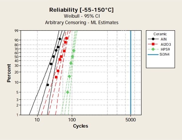
Figure 1c: Lifetime properties of substrates

Figure 1d: Comparison of AMB substrates’ thermal resistance
TIM exhibits very low heat conductivity compared to other structural materials used in power modules, so the TIM layer has to be as thin as possible. TIMs consist of a soft matrix typically made of polymers and a highly heat-conductive solid material. These thermal interface materials have to fill the minute pockets below the power module so the solid material’s grains have to be fine and the ratio of matrix and solid material has to be optimized for flow capability. TIMs’ heat conductivity can be improved with highly conductive solids such as metals and a phase change matrix that makes the most of latent heat between the solid and liquid phase. Comprised of an aluminum solid and phase-change matrix material, PSX-P TIMs are four times more heat conductive than P12 TIMs made of ceramic solid material and a non-phase change silicone matrix.

Figure 2: Rth measurement before and after heat treatment and retightening

Figure 3: Comparison Table
The PSX-P TIM, a solid material, is attached to the backside of the power module and heat treatment is applied after it is fastened in place. The torque on the screws may decrease as the spreading material fills tiny pockets in the honeycomb structure and the TIM layer gets thinner. Hence, the heat treatment and subsequent retightening of screws entails a much greater handling effort.
Easy handling is one of the three priorities, so Rth measurements were taken to assess the effect of heat treatment and retightening. The results indicate that Rth is stable before and after spreading and retightening at the lower and upper torque limits. The solid TIM with the honeycomb structure is thrust up against the heat sink so it touches the surface, creating a thermal bridge that assures heat conductivity. The spreading starts when the power module is first used, but it improves the Rth only slightly because the pockets are so small. The TIM’s thickness decreases after spreading, causing the screws to loosen, but the distance in the small gap between the module and heat sink is kept by the matrix’s surface tension.
A MiniSKiiP® design with a Si3N4 AMB with 0.3, 0.32 and 0.3 mm layers and PSX-P phase change TIM exhibits better thermal resistance and lifetime properties, while remaining just easy to handle an Al2O3 DCB with 0.3, 0.38 and 0.3mm layers and P12 TIM. And that makes it an appealing proposition for customers.
About the Author
Vince Botyánszki works as the Technology Development Engineer at Vincotech, Hungary where he is responsible for Direct Copper Bonded (DCB) or Direct Bonded Copper (DBC) substrates, soldering and washing, as well as housing. He is particularly skilled in the field of semiconductors, power electronics and research and development. He earned his Master's Degree in Information technology in Chemistry at the University of Pannonia located in Veszprém, Hungary.
References
- 2013 Vehicle Technologies Annual Merit Review and Peer Evaluation Meeting Arlington, VA 14 May, 2013 - Low-Cost Direct Bonded Aluminum (DBA) Substrates, H. –T. Lin, A. A. Wereszczak, and S. Waters Oak Ridge National Laboratory
- ECPE – Workshop, Power Electronics Substrates - Materials, Performance, Processing and Reliability, 17 – 18 June 2010, Munich, Germany - Direct Bonded Copper (DBC) Substrates: Status & Potential, K. Exel / A. Meyer, Curamik
- ECPE – Workshop, Power Electronics Substrates - Materials, Performance, Processing and Reliability, 17 – 18 June 2010, Munich, Germany - Si3N4 AMB Substrates for Power Electronics, M. Nagata / C. Yoneda, Kyocera
- Courtesy of Rogers Curamik'
- http://www.kyocera.eu/index/products/microelectronic_packages.- cps-000111-File.cpsdownload.tmp/Kyocera%20-%20Inverter%20 Converter%20Ceramic%20Substrate.pdf