Facebook
 Google
 GitHub
 Linkedin
Investigating Losses of GaN-HFETs in a Synchronous Buck Converter
This article illustrates a thermal measuring method and electrical method with air-core inductors to investigate the losses in eGaNTM FETs.
When a new semiconductor material is introduced into an important area of electrical engineering this raises expectations of business and industry but at the same time can be a significant challenge for manufacturers. After gallium nitride was used for the first time 20 years ago as a transistor and has been used in radio frequency technology for more than a decade, it now conquers power electronics.
The unique material properties of gallium nitride, such as the high electron mobility and saturation velocity as well as the high layer carrier concentration and the high breakdown voltage, propose a superior device performance. This enables operation at high switching frequencies and junction temperatures in power electronics applications. Thus, GaN technology has a superior potential to overcome the performance limitations of silicon semiconductors.
Electrical circuit with EPC2010 eGaN® HFETs
EPC2010 eGaN® HFETs were chosen for these investigations. The transistors have a lateral structure with a hetero-junction between an AlGaN-layer and a GaN-layer in which a two-dimensional electron gas forms, which is responsible for the high electron mobility [1]. The unique characteristic of this structure is the capability to conduct in both directions. Therefore, GaN HFETs do not need a commutation diode, because this function is integrated due to the special structure and characteristics of the materials GaN and AlGaN. Originally, GaN-based HFETs are normally-on switches as the twodimensional electron gas (2DEG) conducts without a voltage applied between the gate and the source. Due to an additional p-GaN layer under the gate, which interrupts the 2DEG, it is possible to create enhancement mode power transistors. EPC2010 eGaN® FETs have a breakdown voltage of 200 V and enable rapid switching, due to their low input capacitance and internal gate resistance [2]. Due to the absence of a PN junction in lateral AlGaN/GaN structures, there is no reverse recovery charge and therefore no delay in these transistors. They can, therefore, be implemented in topologies such as a synchronous buck converter without a freewheeling diode.
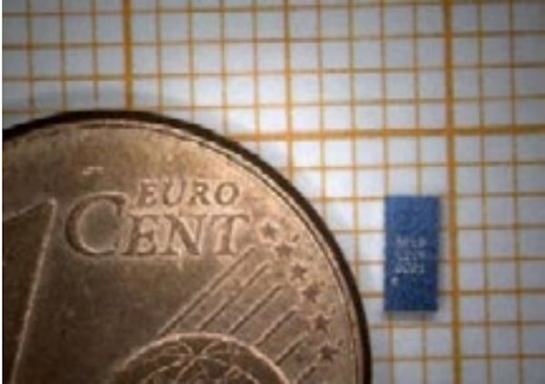
Figure 1: GaN-HFET EPC2010 compared with 1 Cent coin
Since the investigated low-voltage GaN HFETs have no common package as it is the case for conventional semiconductors (Figure 1), it is difficult to realize conventional current measurement. In a practical example of a synchronous buck converter, two experimental methods to determine the power losses in EPC 2010 eGaN HFETs are evaluated.
Asynchronous converter topology with a half-bride was chosen for the investigations (Figure 2). The behavior of the transistors was investigated for hard switching operation with different switching frequencies, input voltages, and output currents.

Figure 2: Synchronous converter topology with a half-bridge using two AlGaN/GaN-HFETs (T1 and T2)
The evaluation board EPC9003 with two 200V EPC2010 eGaN HFETs was used in this electrical circuit. The DC-link consists of a film capacitor of 3.3µF and three ceramic RF-capacitors of 330 nF each. The driver provides a bootstrap circuit with a low gate on-resistor and no gate off-resistor. Several inductors, built with magnetic cores from different materials, were used as output chokes with inductance values between 100µH and 500µH. These values were calculated from the initial parameters and test conditions which were:
- 100V input voltage
- output current from 0.5A to 2A with 0.5A ripple current
- 0.5 duty cycle
- switching frequencies from 100kHz to 500kHz in 100kHz steps
Experimental methods of investigating the power losses
To estimate, where the limits of the switching frequency of the semiconductors are in terms of the switching power losses, conventional methods use current and voltage measurements during the commutation period. The conventional current measurement is based on the induction of a magnetic field, caused by the flowing current (current sensor) or on measuring the voltage drop across a resistance built in the drain-source path (shunt). However, an accurate measurement of the drain current of the EPC GaN HFETs with the conventional current measurement is not suitable. Any such measurements (sensors, shunts) cause additional leakage inductance. Due to the small size, the EPC GaN HFETs have extremely low internal leakage inductance, which is significantly less than the leakage inductance of an external component for current measurement. For this reason, the measurements of the drain-source current in EPC GaN HFETs, using conventional current sensors or shunts, would not provide meaningful results.
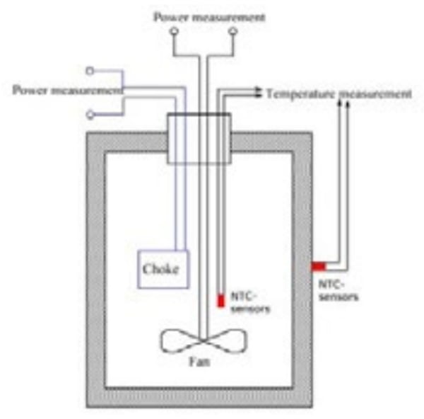
Figure 3: Schematics of the calorimeter to determine the power losses in the output choke
Nevertheless, the losses in these unusually tiny power transistors can be determined indirectly without actually measuring the drain current. The suggested method is based on the measurement and determination of the remaining losses in an electrical circuit and, after that, a calculation of the semiconductor’s losses, which are the only losses that cannot be determined directly by experimental tests.
Measurements with a calorimetric method
The total power losses of the entire circuit were measured with a power meter (analyzer) ZES ZIMMER as well as with multimeter and oscilloscope. The losses in the output choke were determined by means of the inertia calorimeter principle (Figure 3 and Figure 4).
In order to calculate the power losses in the chokes eight NTC-sensors were used: four inside and four outside the thermally insulated container, to monitor the temperatures. It was investigated which core material was most suitable for each of the applied frequencies and currents. Conclusions were drawn regarding the usability of the magnetic components operating at high frequencies (in terms of power electronics). Three magnetic core materials were chosen for the investigation: ferrite MnZn (3C20) as well as powder (AmoFlux and 3W7538). Fourteen chokes were built up, using the selected materials, for different switching frequencies.
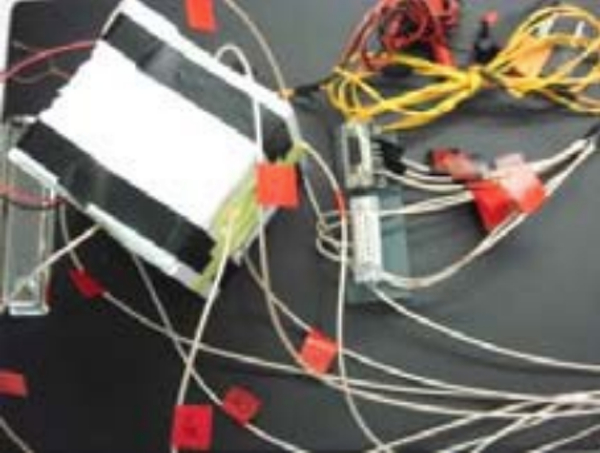
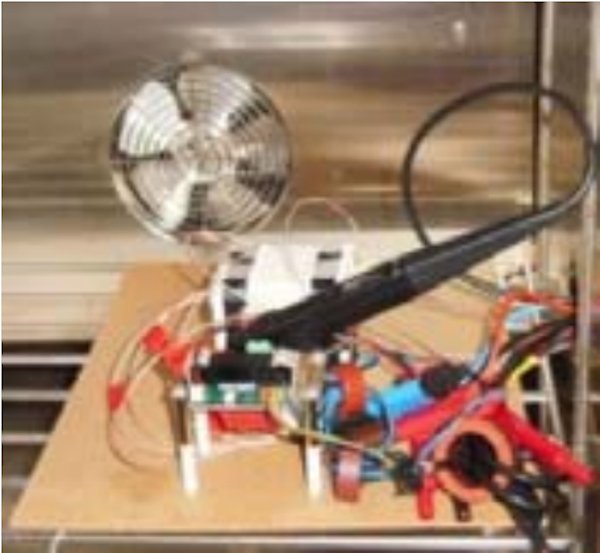
Figure 4: Calorimeter set-up for analysis of the power losses in the output choke with sensors and terminals
The efficiency of the circuit was investigated with various output chokes which were designed as toroids from different magnetic core materials.
The losses of the chokes were calculated by using the formula [3]:
The time derivative of the temperature was assumed to be negligible, as the time for each measurement was long beyond the thermal equilibrium. The thermal resistance was determined by means of reference measurements with several load resistors.
Measurements by means of air coils
The disadvantage of the calorimetric method is the considerable period of time for any single measurement and inaccuracies caused by temperature measurements of different chokes. The disadvantage of using chokes with ferromagnetic cores is the non-linearity of magnetic materials. Therefore, the determination of the losses in a choke with ferromagnetic core is more complicated and less accurate than in an air-core coil. Several air-core chokes with low capacitance, such as basket coils (Figure 5; left) or cross-wound coils (Figure 5; right), were assembled for different switching frequencies. Using these chokes, the power losses may be determined easier.

Figure 5: Low capacitive air-core coils
![Power losses in GaN semiconductors at different switching frequencies; circuit operated at different frequencies with three chokes (3c20, 3W7538, and AmoFlux) at 100 W output power [5].](https://eepower.com/uploads/thumbnails/2020-4805-hamburg-university-applied-sciences-university-kassel.jpg)
Figure 6: Power losses in GaN semiconductors at different switching frequencies; circuit operated at different frequencies with three chokes (3c20, 3W7538, and AmoFlux) at 100 W output power [5].
![Power losses in the eGaN-HFETs and their approximation as a function of the switching frequency at 100 V input voltage and four different output currents [5].](https://eepower.com/uploads/thumbnails/2020-4804-hamburg-university-applied-sciences-university-kassel.jpg)
Figure 7: Power losses in the eGaN-HFETs and their approximation as a function of the switching frequency at 100 V input voltage and four different output currents [5].
Results
The chokes with 3C20 and AmoFlux magnetic cores feature a higher efficiency over the entire tested frequency range and can be used in a circuit with eGaN® FETs. However, it must be considered that not only semiconductors, but also the magnetics exhibit limits regarding power density [4]. The power losses in the GaN semiconductors are determined from the losses of the whole circuit and the ascertained power losses in the chokes. The driver losses are also considered. The losses in other components and conductors were found to be negligible at output powers of 100 W or less. As Figure 6 shows, the power losses in the GaN semiconductors are similar regardless of the choke used.
In the measurements with the air-core coils, the power losses in the eGaN-HFETs were calculated, after the total losses of the circuit were determined and other losses such as winding losses had been subtracted (Figure 7).
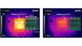
One interesting fact from these measurements is that – at relatively low current levels (e.g. 0.5 A) – the total losses rise steeper with increasing switching frequency than at a current level significantly higher (e.g. 2 A). This tendency was also observed during tests with infra-red thermal imaging (Figure 8). Losses of the two transistors increase at different rates. It can be observed that the temperature in the top transistor (T1) rises, as expected, with increasing current and increasing frequency. In the bottom transistor (T2) the conditions are different. This transistor is soft-switching. Not only increases the temperature along with the frequency at a steeper rate when the current is low, but the absolute figure of dissipation in the bottom transistor is higher at 0.5 A than at 2.0 A for frequencies above 100 kHz (see Figure 8).
![Temperature gradients for different currents at different frequencies split for top (T1) and bottom (T2) transistors [5]](https://eepower.com/uploads/thumbnails/2020-4803-hamburg-university-applied-sciences-university-kassel.jpg)
Figure 8: Temperature gradients for different currents at different frequencies split for top (T1) and bottom (T2) transistors [5]
![Power loss dependency of the eGaN-HFETs with 100V input voltage and currents up to 5A for different frequencies [5]](https://eepower.com/uploads/thumbnails/2020-4802-hamburg-university-applied-sciences-university-kassel.jpg)
Figure 9: Power loss dependency of the eGaN-HFETs with 100V input voltage and currents up to 5A for different frequencies [5]
Initially, this seems paradoxical. However, it is due to the fact that the frequency-dependent losses, attributable to changing the charge status of the transistors, are a) dominant for smaller output currents and b) distributed very asymmetrically. More specifically: One important factor for the current charging and discharging the output capacitance of the upper transistor is the load impedance. A high impedance (i.e. low load current) will let a greater proportion of the charge/discharge current be taken up by the bottom transistor. This is a major contributor to the dissipation and thus heating of T2. As the load is increased (i.e. the load impedance decreases) a greater proportion of the top transistor’s charge/ discharge current flows through the load path and thus mitigates the dissipation of the bottom transistor. Once the current reaches approximately 2 A, the increasing conduction losses become dominant. This apparent inconsistency is a less important fact when designing a synchronous buck converter with these specific devices used, as it occurs only when operating at very low load. The settings of the interlock delay times (dead times) play a decisive role in this.
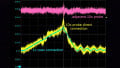
Finally, the EPC 2010 eGaN® HFETs were tested at currents up to approx. 5 A and at frequencies of 220 kHz, 315 kHz and 410 kHz (Figure 9).
For this, air-core inductors were wound with RF-Litz wire appropriately sized for the current. The frequencies were chosen accordingly so that the ripple current was 0.5 A, as with all other measurements. The dotted lines in the diagram (Figure 9) indicate the trend lines between the measured points. At all frequencies, there is a current dependence, which can be described with a polynomial of the second degree. This, in turn, means that the change in the power losses at any frequency is determined primarily by the conduction losses, which are entered into the equation as a square function.
The semiconductor losses at 5 A are approximately 2.5% at 220 kHz and 2.8% at 410 kHz accordingly. With a calculated design of the magnetic components, adequate cooling and an appropriate circuit board design, an efficient and compact synchronous buck converter with EPC eGaN-FETs is thus possible.
Conclusion
Undoubtedly the eGaN-HFETs are suitable for operation in high-frequency switching applications. However, several points can be discussed in more detail. Hard switching will cause limitations regarding the combination of the magnetic core material and losses occurring due to the switching action itself. Depending on the application there will be an optimum frequency, where the losses drop to a minimum depending on the combination of the semiconductors and magnetic components. A further frequency increase may allow downsizing of the filter components in the circuit even more, whilst higher semiconductor losses must be suffered. If, therefore, an excessive frequency increase is required, the application of soft switching circuits and resonant methods should be considered.
One further issue is the optimization of specific operating values. Namely, the interlock delay times, the leakage inductances of the various circuit parts, balancing of inductive and capacitive components (both real and leakage), setting up of a suitable control function for the duty cycle, to mention just some.
About the Authors
Marita Wendt works as a Scientific Associate at The Hamburg University of Applied Sciences (HAW Hamburg), Germany, an institution of higher education and applied research located in Hamburg, Germany. Formerly known as Fachhochschule Hamburg the Hamburg University of Applied Sciences was founded in 1970.
Thiemo Kleeb and Peter Zacharias both work as professors at the University of Kassel, Germany, a university founded in 1971 located in Kassel, Hessen, in Germany. As of October 2013, it had about 23,000 students and more than 2,600 staff, including 307 professors. Mr. Kleeb belongs to the Centre of Competence for Distributed Electric Power Technology (KDEE), while Mr. Zacharias is assigned at the Institute of Electrical Power Engineering (IEE).
This article originally appeared in the Bodo’s Power Systems magazine.