 Facebook
 Google
 GitHub
 Linkedin
How 150 V Silicon Power MOSFETs Expand Synchronous Rectifier Options in AI Servers
Using a 5.5 kW, 54 V supply as a case study, this article examines how low-resistance 150 V silicon MOSFETs can enable a simpler center-tapped secondary with fewer devices and a smaller rectifier footprint.
This article is published by EEPower as part of an exclusive digital content partnership with Bodo’s Power Systems.
AI platforms have driven server power supply output well beyond the 3.3 kW to 5.5 kW levels that were once considered high-end, with rack power densities continuing to climb as GPU and ASIC compute density increases. These demands put greater pressure on secondary rectifier size, component count, and cost. At a fixed output voltage, higher power requires proportionally higher current, making MOSFET selection and rectifier topology closely linked design decisions.
Using a 5.5 kW, 54 V supply as a case study, this article examines how low-resistance 150 V silicon MOSFETs can enable a simpler center-tapped secondary with fewer devices and a smaller rectifier footprint. The potential cost and space savings become even more significant across the tens of thousands of power supplies deployed per data center.

Image used courtesy of Freepik
The Secondary Side Becomes a Design Priority
Delivering 5.5kW at 54V requires approximately 102A of continuous output current. At that operating point, secondary rectification becomes a substantial design task. MOSFET resistance affects conduction loss, while the number and arrangement of devices determine how much board space, gate-drive circuitry, and thermal infrastructure the stage requires.
Paralleling low-resistance MOSFETs is one way to handle the current. However, each additional device also needs space, electrical connections, and a layout that supports appropriate current sharing. The resulting implementation can consume a significant portion of the available secondary-side area. For designers seeking higher power density, reducing that footprint creates an opportunity to reconsider how the power stage is built.
Advances in 150V silicon make this question particularly relevant to 54V supplies. Higher-voltage MOSFETs with low on-resistance can support a center-tapped rectifier using fewer devices than the full-bridge implementation considered here. A 5.5kW case study shows how that choice affects the physical implementation and semiconductor bill of materials.
How Silicon Performance Changes the Topology Tradeoff
Full-bridge and center-tapped synchronous rectifiers impose different requirements on their MOSFETs. A full-bridge secondary uses a bridge arrangement to rectify the transformer output. Its conducting current path includes two switch positions in series. Parallel MOSFETs at each position reduce the resistance presented to the current.
A center-tapped secondary uses two winding sections that conduct on alternate half cycles. Each active current path passes through one rectifier switch position. This arrangement can reduce the number of MOSFETs needed, but it places greater blocking-voltage demands on those devices. For comparable output conditions, center-tapped rectification exposes the off-state devices to approximately twice the secondary voltage of the full-bridge arrangement, before accounting for ringing and design margin.
The traditional challenge has been obtaining sufficiently low resistance at that higher voltage rating. The attraction of eliminating a series switch position can diminish if the required higher-voltage MOSFET introduces excessive resistance. Improvements in 150V silicon directly address this constraint, allowing designers to achieve low effective rectifier resistance with fewer parallel devices, as shown in Figure 1.
The relevant comparison therefore includes both the MOSFET characteristics and the current path created by the topology. Low on-resistance remains central to the result: better performance at the required blocking voltage gives designers more freedom to simplify the circuit.
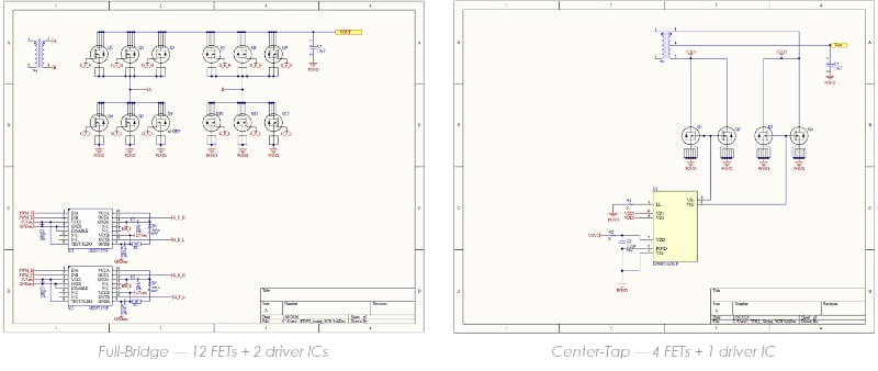
Figure 1. Full-bridge and center-tapped secondary schematics. The center-tap topology enables 71% fewer key components. Image used courtesy of Bodo’s Power Systems [PDF]
Two Implementations at 5.5kw, 54V for AI Power Supplies
As shown in Table 1, the case study compares secondary rectifiers at 5.5kW output, 54V output voltage, and 100kHz switching frequency. It uses a half-sine rectifier-current model with approximately 160A peak current. The common operating point provides a basis for examining the consequences of the secondary implementation.
Table 1. 5.5kW AI server power supply converter specifications
| Parameter | Value | Unit |
| Output Power | 5500 | W |
| Output Voltage | 54 | V |
| Output Current | 101.9 | A |
| Switching Frequency | 100 | kHz |
| Half-Sine Peak Current | 159.9 | A |
| Half-Sine RMS Current | 79.9 | A |
The full-bridge option uses twelve 80V MOSFETs and two gate-driver ICs. The center-tapped option uses four 150V MOSFETs and one gate-driver IC. Component counts and occupied rectifier PCB areas come from representative schematic and layout implementations. The loss analysis uses rated on-resistance, while the cost comparison uses assumed high-volume prices for the MOSFETs and driver ICs.
These boundaries matter. The comparison quantifies the rectifier implementation and its semiconductor cost. It does not establish a complete power supply cost or efficiency result. In particular, you must evaluate transformer winding differences, switching losses, and operating temperature when developing the complete converter.
Fewer Devices With Low Effective Resistance
The selected 80V devices, Infineon’s ISC014N08NM6 and ISC018N08NM6SC, have maximum on-resistance values of 1.45mΩ and 1.80mΩ, respectively. With three devices in parallel at each switch position and two positions in the conducting path, the resulting path resistance is approximately 0.97–1.20mΩ. The 150V device, iDEAL Semiconductor’s SuperQ® iS15M2R5S1T, has a maximum on-resistance of 2.5mΩ. Two devices in parallel at each center-tapped rectifier position produce a conducting-path resistance of 1.25mΩ.
This comparison explains why the reduction from twelve MOSFETs to four is possible without a proportionate increase in effective resistance. Although the 150V devices must support a higher blocking voltage, the topology removes one series switch position from the conducting path. The low resistance of the selected 150V devices then keeps the resulting path resistance close to the full-bridge alternatives.
The reduction is substantial: eight fewer MOSFETs, or approximately 67%. The selected center-tapped implementation also consolidates gate drive into one IC instead of two. The reduced supporting circuitry also improves layout.
Board Space and Semiconductor Cost
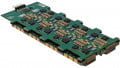
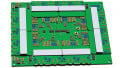
As shown in Figure 2, the full-bridge layout occupies approximately 1,785 mm², compared with 782 mm² for the center-tapped implementation, a reduction of approximately 56%. This is the occupied area of the secondary rectifier implementation, including the layout around its components.
The distinction between package area and implementation area is instructive. The center-tapped option uses larger TOLL packages, whereas the full-bridge option uses 5 × 6 mm PDFN packages. The combined MOSFET package area is actually slightly larger for the center-tapped option. Nevertheless, the complete rectifier layout is considerably smaller. The number and arrangement of switch positions, driver circuitry, spacing, and interconnections influence the occupied board area beyond the sum of the package footprints.
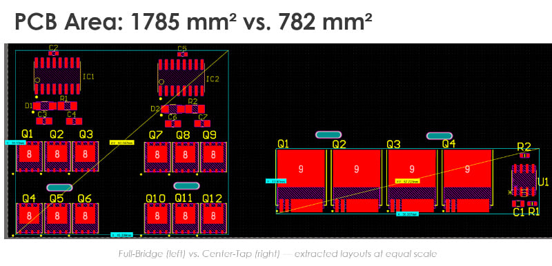
Figure 2. Full-bridge and center-tapped secondary rectifier layouts shown at equal scale. Image used courtesy of Bodo’s Power Systems [PDF]
The semiconductor cost comparison follows a similar pattern. Using the lowest-cost device option in each topology, the full-bridge MOSFETs cost $9.60, and the driver ICs cost $2.00, for a combined $11.60. The center-tapped MOSFETs cost $7.20, and their driver ICs cost $0.50, totaling $7.70. The difference is $3.90 per supply, or approximately 34%, under the case study’s pricing assumptions, shown in Table 2.
For a power supply manufacturer, these results identify specific opportunities: a smaller secondary rectifier footprint, fewer semiconductor placements, and lower MOSFET-plus-driver expense.
Table 2. Secondary rectifier implementation comparison
| Metric | 80V full bridge | 150V center-tapped |
| MOSFET count | 12 | 4 |
| Gate-driver IC count | 2 | 1 |
| Equivalent conducting-path resistance | 0.97–1.20mΩ | 1.25mΩ |
| Rectifier PCB area | 1,785 mm² | 782 mm² |
| MOSFET and driver cost¹ | $11.60 | $7.70 |
¹ Lowest-cost option for each topology using the case study’s assumed volume pricing. Transformer and other converter costs are excluded.
Efficiency Evaluation and Design Tradeoffs
Although the center-tapped implementation uses fewer MOSFETs, the rectifier current remains the same. Each 150V MOSFET has approximately twice the on-resistance of an 80V device and therefore dissipates more conduction power individually. In the full-bridge topology, comparable loss is distributed across two 80V MOSFETs in the conduction path, resulting in similar total conduction loss for the two topologies.
At full load, efficiency loss ranges from 0.056%–0.070% for the full-bridge devices versus 0.073% for the center-tapped devices, a difference of roughly 0.02%. At 50% load, the gap narrows to about 0.004%. In practical terms, the center-tapped topology delivers a 71% component-count reduction and a 56% area reduction with a minimal conduction-loss penalty for most system-level efficiency targets.
Realizing these space and component savings also requires attention to thermal management, current sharing, and performance across operating conditions. Using four larger MOSFETs instead of twelve smaller devices concentrates heat, potentially requiring changes to copper area, thermal vias, or heatsinking.
Fewer parallel devices simplify current sharing and reduce solder joints and gate-drive connections but increase per-device current and thermal demands. The smaller rectifier footprint offers opportunities for higher power density, although scaling depends on cooling and device ratings. Final designs should verify conduction and switching losses across operating temperatures, loads, and transients rather than relying solely on RDS(on) estimates.
A Practical Opportunity for Power Supply Designers
This case study illustrates how low-resistance 150V silicon MOSFETs can expand designers’ options for secondary rectification. Compared with the selected full-bridge implementation, the center-tapped approach uses 67% fewer MOSFETs, occupies 56% less rectifier PCB area, and reduces assumed MOSFET and driver cost by 34%.
These advantages make it worth evaluating where space and component count are priorities, with the final choice determined by transformer requirements, thermal performance, and complete converter losses. As AI server power density and cost pressures increase, evaluating topology and device selection together becomes essential to achieving a more compact, cost-effective power supply.
This article originally appeared in Bodo’s Power Systems [PDF] magazine.