Facebook
 Google
 GitHub
 Linkedin
Buffer Technology Improves Fast Recovery Diodes for High-Speed IGBTs
This article deals with fast recovery diodes (FRDs), which are tailored for high-speed IGBT applications, aiming to reduce oscillations, voltage overshoot, and electromagnetic interference (EMI) while maintaining soft reverse recovery and low losses.
This article is published by EEPower as part of an exclusive digital content partnership with Bodo’s Power Systems.
Article co-authored by StarPower Semiconductor's Hua Shen, Fu Yong, Rebecca Li and Bruce Chen.
StarPower Semiconductor has developed a high-voltage diode technology featuring smooth recovery behavior and an increased safe operating area (SOA). By optimizing anode and buffer implantation doses, the diodes achieve lower positive temperature coefficients and reduced hot-state leakage current. Experimental results align well with numerical models.
The design also incorporates a Varied Lateral Doping (VLD) termination, combined with SIPOS, SiN, and polyimide passivation, to minimize termination area while approaching ideal parallel-plane breakdown voltage. These fast recovery diodes (FRDs) are tailored for modern, high-speed IGBT applications, aiming to reduce oscillations, voltage overshoot, and electromagnetic interference (EMI) while maintaining soft reverse recovery and low losses.

Image used courtesy of Freepik
Recently, novel cathode structures have been proposed as the most effective approach to achieving soft recovery behavior in high-voltage diodes. Additionally, to ensure a large safe operating area (SOA), the diodes must be free from design weaknesses in both the active regions and the chip edge termination [1–14].
The next generation of high-voltage diodes must exhibit high dynamic robustness and support safe turn-off under high voltage and high di/dt test conditions. Increasing the thickness of the Ndrift layer is one potential solution, but it leads to higher overall losses. While existing diode technologies offer promising soft recovery and SOA performance, they face limitations in terms of forward voltage drop (Vf), total losses, soft recovery behavior, and SOA.
Overcoming these limitations is essential to fully realize their potential. Consequently, developing next-generation high-voltage diodes that combine the high performance of fast-switching IGBTs with low losses is critical for overall system efficiency. This work presents a practical analysis of conventional and newly proposed cathode structures. The proposed design shows promising results for future high-voltage diodes.
Structure
Figure 1 shows a simplified cross-section of the proposed VLD (variation of lateral doping) structure, which includes a buried boron layer within the N-buffer region. The structure is fully compatible with IGBT process technology. To ensure consistency with process conditions, the structure was defined directly using DIOS and subsequently simulated with TCAD software [15]. Particular care was taken to achieve close agreement between measured and simulated propagation resistance profiles.
Since SIPOS (semi-insulating polycrystalline silicon) is a semiconducting layer and difficult to implement in breakdown voltage simulation tools, a zero-charge assumption was adopted for VLD structure optimization. A hydrogen buffer layer and a buried P-layer were incorporated to enable soft recovery and enhance SOA capability under severe switching conditions. To reduce hot-state leakage current, electron irradiation was used exclusively, while the boron dose at the anode controls the hole injection efficiency into the drift region.
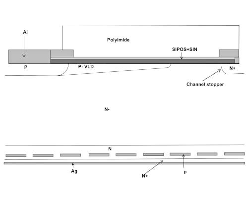
Figure 1. Cross section of a proposed FRD structure. Image used courtesy of Bodo’s Power Systems [PDF]
VLD termination is based on implantation through small openings in the oxide using a photoresist mask and subsequent drive-in to achieve a controlled doping profile as shown in Figure 1. The main advantage of VLD termination lies in the reduced termination area, as the depletion zone extends completely to the surface and shares the potential with the substrate. For a given chip size, the anode area can be increased to reduce Vf and increase the surge current.
However, the structure is sensitive to surface charges and therefore requires good passivation, e.g., with SIPOS or DLC, to achieve a stable breakdown voltage or to pass reliability testing. The IGBT modules used are GD1000MPA140L8S and GD1000MNA140L8S, 1000 A, 1400 V modules with three FRDs connected in parallel.
Analysis of Switching
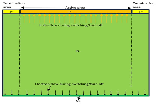
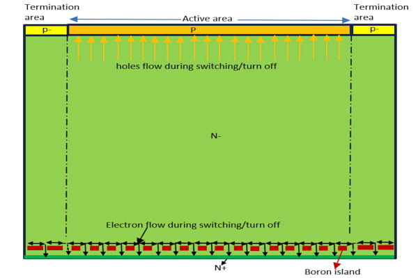
In order to study switching behavior under reverse bias operation, a practical reverse recovery test is performed using two structure types shown in Figure 2 with and without a boron buried layer or Controlled Injection of Backside Holes (CIBH). The devices have seen VLD termination, achieving a static breakdown voltage of 1550 to 1600 V.
Due to breakdown at the boron island and the N+ junction in the cathode region, the leakage current of the CIBH diode is higher than that of conventional diodes. Since several diodes are connected in parallel in a module, this leakage current must be reduced. The avalanche at this junction is adjusted by optimizing the boron dose and ratio between P and N buffer layers to prevent a significant increase in leakage current.
Figure 3 illustrates Vf of diodes with and without CIBH at 25 and 150 °C. Measurement results show that both have similar Vf: 2.45 V at RT and 2.8 V at 150 °C, respectively. During turn-off, the complete drift area is flooded with free carriers, while in the CIBH diode, boron areas are in parallel direction, so Vf is not significantly affected (maximum Vf reduction: 0.1 V).
with CIBH
without CIBH
Figure 2. Schematic diagram of FRD with and without CIBH during turn-off. Image used courtesy of Bodo’s Power Systems [PDF]
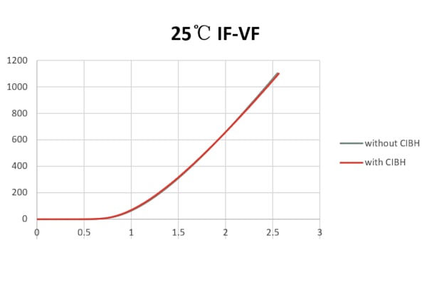
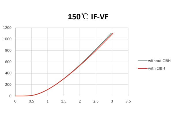
Figure 3. Forward voltage drops at RT and 150 °C. Image used courtesy of Bodo’s Power Systems [PDF]
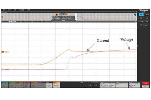
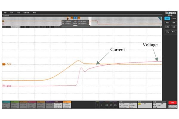
Figure 4 shows the switching and recovery waveforms of the device shown in Figure 2. The devices were switched at a bias voltage of 800 V, 4600 A/µs, 1200 A, 95 nH with gate resistance of 10 Ω at RT. Devices with and without CIBH show soft recovery.
with CIBH
without CIBH
Figure 4. Switching waveform with gate resistance of 10 Ω with and without CIBH at 25 °C at 1200A. Image used courtesy of Bodo’s Power Systems [PDF]
Table 1. Switching loss at RT with gate resistance of 10Ω.
|
|
With CIBH 25°C |
Without CIBH 25°C |
|
di/dt (test condition) |
4610 |
4710 |
|
Inductance |
95nH |
95nH |
|
Qrr |
48.11 |
52.02 |
|
Irrm (A) |
206 |
266 |
|
Vrp (V) |
767 |
764 |
|
Trr (ns) |
275 |
284 |
| As per the switching waveform | |
|
Voltage/division (Y axis) |
200 |
|
Current/division (Y axis) |
500 |
|
Trr /division (X axis) |
400ns |
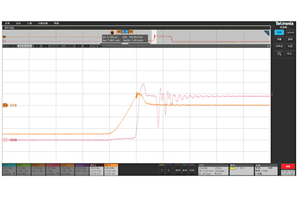
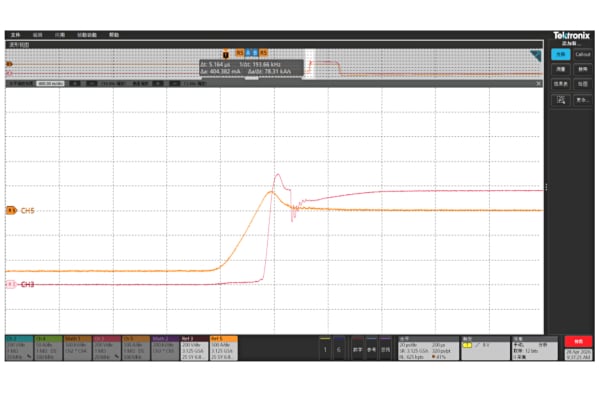
As the gate resistance is reduced to 6.8 Ω, losses increased as shown in Table 2, with di/dt increasing to 7200 A/µs. During reverse recovery, the reference diode shows voltage oscillations as in Figure 5. With gate resistance decreasing, the switching speed of di/dt increases. Since there are fewer holes in the base region, the occurring oscillations are clearly visible in the voltage spikes (Vrp). Using CIBH with boron on the cathode side improves the softness, as buried p-doped areas inject holes into the base region. Furthermore, Irrm decreases, and the voltage overshoot is reduced.
Table 2. Switching loss at RT with gate resistance of 6.8 Ω at 1200 A.
|
|
With CIBH 25°C |
Without CIBH 25°C |
|
di/dt(test condition) |
7230 |
7340 |
|
Inductance |
95nH |
95nH |
|
Qr |
57.67 |
77.46 |
|
Irrm (A) |
395 |
505 |
|
Vrp (V) |
900 |
982 |
|
Trr (ns) |
240 |
217 |
without CIBH
with CIBH
Figure 5. Switching waveform with gate resistance of 6.8 Ω with and without CIBH at 25 °C. Image used courtesy of Bodo’s Power Systems [PDF]
During reverse recovery, an electric field builds up on the cathode side of the diode between the NN+ junctions. It is reduced by hole injection into the CIBH diode. This process leads to increased softness, as the reverse recovery time (trr) increases from 217 ns to 240 ns, the voltage overshoot remains below the diode’s breakdown voltage, and robustness improves.
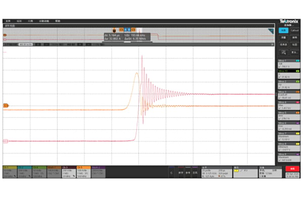
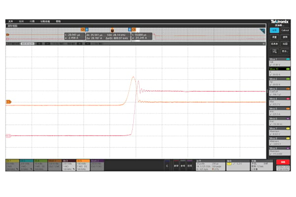
To verify the low-current switching behavior, the devices were switched off at an initial forward current of 20 A and 100 A of a 1000 A module, with the gate resistance held constant at 6.8 Ω and the module inductance at 95 nH. Since low-current test conditions provide a better understanding of the switching results, the switching diagrams at 20 A are shown in Figure 6 at 150 °C.
The waveform clearly demonstrates that without buried P layers, devices show snappy behavior, and Table 3 clearly shows that the voltage overshoot Vpk is much higher than in devices with buried P layers. An increase in buried layer Boron concentration helps in reducing oscillations further; however, Vf and leakage current increase. A suitable balance must be found between an acceptable fast switching behavior and a completely smooth switching behavior, taking static losses into account.
The improved, smoother recovery allows the diode to operate at higher di/dt values and current densities without failure. To verify the RRSOA capability of a module, the devices were switched at 2500 A (2.5 times the rated current) and a bias voltage of 800 V with a gate resistance of 6.8 Ω. All module samples passed the same test at room temperature and 150 °C.
Table 3. Switching loss at RT with gate resistance of 6.8 Ω at 20 A.
|
|
With CIBH 150°C |
Without CIBH 150°C |
|
+di/dt (test condition) |
2880 |
2940 |
|
Inductance |
95nH |
95nH |
|
Qr |
25.16 |
29.87 |
|
Irrm (A) |
226 |
279 |
|
Vrp (V) |
974 |
1457 |
|
Trr (ns) |
223 |
192 |
without CIBH
with CIBH
Figure 6. Switching wave form with gate resistance 6.8 Ω with and without CIBH at 25 °C at 20 A. Image used courtesy of Bodo’s Power Systems [PDF]
Reliability
VLD termination is used to obtain the highest possible breakdown voltage. When the device is in avalanche, breakdown voltage VLD completely depletes to the surface; therefore SIPOS passivation is used to obtain a stable breakdown voltage. SIPOS is deposited directly on the silicon surface because it has got limited conductivity. Any undesired charge such as ionic contamination, interface or trapped charges which may disturb the electric field distribution is compensated by mobile carriers within the SIPOS. The LPCVD machine deposits 0.2 µm of SIPOS with SIN passivation. Conductivity of SIPOS is carefully adjusted by oxygen content during deposition.
Prior to the official production release the devices went through full qualification testing. The most important reliability tests for the electrical stability of the chip are High Temperature Reverse Bias (HTRB) and humidity test. The HTRB test checks the ability of the samples to withstand a reverse bias while being subjected to the maximum ambient temperature that the parts are rated to withstand. The condition used for the HTRB test is 80 % of the rated voltage at 150 °C. The breakdown voltage and leakage current were measured before starting the test. 1400 V 156 chips were assembled into the C6 package. The test was conducted for up to 1000 h and readings were observed once every 8 hours. Pre and Post measurement results showed there is no increase in leakage current.
Humidity test checks the ability of the package and chip to resist moisture penetration. The sample is loaded into an environmental chamber. The relative humidity is then increased 85 % and the temperature is elevated to 85 °C. The device characteristics are measured before starting the test. The devices are re measured after cooling down for 3h. Pre and post measurement results show no increase in leakage current.
Conclusion
Simulation analysis and practical results proof that by using a VLD structure and optimised buried boron layer dose it is possible to obtain a breakdown voltage of 1550 V with thin N-thickness of 140 µm. It was practically demonstrated that the controlled injection of backside holes provides a soft recovery diode in comparison to the traditional diode without buried P layer. The reliability results confirm that the use of SIPOS for passivating a planar PN junction leads to stable reverse voltage characteristics.
References
[1] Katsumi Nakamura, Fumihito Masuoka, Akito Nishii, Koji Sadamatsu, Soichi Kitajima and Kazunari Hatade, “Advanced RFC Technology with New Cathode Structure of Field Limiting Rings for High Voltage Planar Diode,” Proc. ISPSD’10, pp133- 136, 2010
[2] J. Lutz and M. Domeij, “Dynamic Avalanche and Reliability of High Voltage Diodes,” Microelectronics Reliability, vol. 43, pp529-536, 2003
[3] Min Chen, Josef Lutz, Martin Domeij, Hans Peter Felsl, HansJoachim Schiulze, “A Novel Diode Structure with Controlled Injection of Backside Holes,” Proc. ISPSD’06, pp45-48, 2006
[4] K. Nakamura, H. Iwanaga, H. Okabe, S. Saito and K. Hatade, “Evaluation of Oscillatory Phenomena in Reverse Operation for High Voltage Diodes,” Proc. ISPSD’09, pp156-159, 2009
[5] H. P. Felsl, M. Pfaffenlehner, H. Schulze, J. Biermann, Th. Gutt, H. –J. Schulze,, M. Chen and J. Luts, “The CIBH Diode – Great Improvement for Ruggedness and Softness of High Voltage Diodes,” Proc. ISPSD’08, pp173-176, 2008
[6] A. Kopta and M. Rahimo, “The Field Charge Extraction (FCE) Diode A Novel Technology for Soft Recovery High Voltage Diodes,” Proc. ISPSD’05, pp83-86, 2005
[7] M. Rahimo, A. Kopta and S. Linder, “Novel Enhanced-Planar IGBT Technology Rated up to 6.5kV for Lower Losses and Higher SOA Capability,” Proc. ISPSD’06, pp33-36, 2006
[8] K. Satoh, K. Morishita, Y. Yamaguchi, N. Hirano, H. Iwamoto and A. Kawakami, “A Newly Structured High Voltage Diode Highlighting Oscillation Free Function in Recovery Process,” Proc. ISPSD’2000, pp249-252, 2000
[9] K. Nakamura, D. Oya, S. Saito, H. Okabe and K. Hatade, “Impact of an LPT(II) Concept with Thin Wafer Process Technology for IGBT’s Vertical Structure,” Proc. ISPSD’09, pp295 298, 2009
[10] J. Lutz, R. Baburske. M. Chen, M. Domeij. H. P. Felsl and H. -J. Schulze, “The nn+-Junction as the Key to Improved Ruggedness and Soft Recovery of Power Diodes,” IEEE Trans. Electron Devices, vol. 56, no. 11, pp2825-2832, 2009
[11] Y. Tomomatsu, E. Suekawa, T. Enjyoji, M. Takeda, H. Kondoh, H. Hagino and T. Yamada, “An Analysis and Improvement of Destruction Immunity During Reverse Recovery for High Voltage Planar Diodes under High dIrr/dt Condition,” Proc. ISPSD’96, pp353-356, 1996
[12] J. G. Bauer, T. Duetemeyer, E. Falck, C. Schaeffer, G. Schmidt and H. Schulze, “Investigations on 6.5kV Trench IGBT and adapted EmCon Diode,” Proc. ISPSD’07, pp5-8, 2007
[13] K. Nakamura, K. Sadamatsu, D. Oya, H. Shigeoka and K. Hatade, “Wide Cell Pitch LPT(II) CSTBTTM(III) Technology Rating up to 6500 V for Low Loss,” Proc. ISPSD’10, in press, 2010
[14] H. Egawa, ”Avalanche Characteristics and Failure Mecha nism of High Voltage Diodes” IEEE Transaction on Electron Devices, Vol. 13, No. 11, November 1966
[15] DESSISISE User manual, SYNOPSYS INC.
This article originally appeared in Bodo’s Power Systems [PDF] magazine and is co-authored by J.V. Subhas Chandra Bose, Hua Shen, Fu Yong, Rebecca Li, and Bruce Chen, StarPower Europe