Facebook
 Google
 GitHub
 Linkedin
From Grid to GPU: Enabling Multi-Megawatt SST Architectures With High-Current SiC Power Modules
AI-driven data centers require power supplies with high efficiency, power density, and reliability. Solid-State Transformer (SST) architectures based on SiC power modules enable direct conversion from 34.5 kV medium-voltage grids to 800 V and future 1500 V data center DC infrastructures. This article highlights how high-power SSTs and high-current, highly reliable SiC modules can support multi-megawatt hyperscaler applications while improving efficiency and the key AI performance metric: “Tokens per Second per Megawatt.”
This article is published by EEPower as part of an exclusive digital content partnership with Bodo’s Power Systems.
Article co-authored by Mitsubishi’s Karthik Debbadi, Nils Soltau, and Ryo Tsuda.
The electricity demand of data centers is set to increase by at least twofold until 2030 [1]. Moreover, large-scale data centers (Hyperscalers) will be a key driver for the overall electricity demand [2]. Today, 72% of the data centers have a power demand of more than 50 MW [3], and blueprints for 100 MW installations are available [4]. Trends indicate that future Hyperscalers demand power in the GW range [5].
Today, electrical power and the connection to the electricity grid are considered to be the ultimate constraint for AI infrastructure [6]. Therefore, “performance per Watt” or “Tokens per Second per Megawatt” are considered key indices for evaluating AI throughput. AI infrastructure is power-hungry, and any improvement in efficiency translates into “tokens” and finally into revenue.
Considering the trajectory of power demand for AI infrastructure and the improvements to “Tokens per Second per Megawatt”, it can be summarized that power supply for AI infrastructure will require solutions that can innovatively combine high power densities and high operational efficiency while maintaining a certain level of modularity to scale output power.
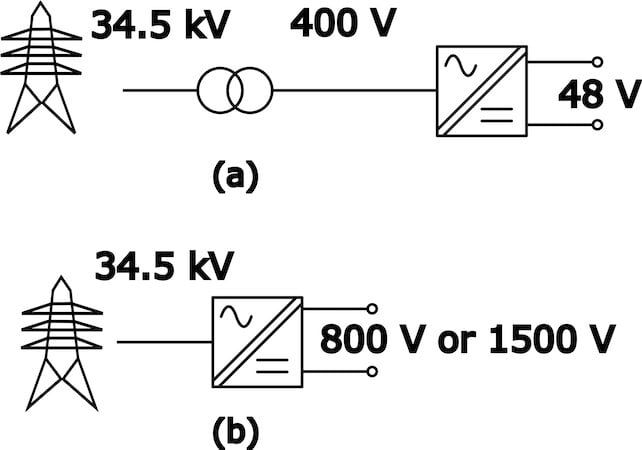
Figure 1. (a) Conventional approach with Low Frequency Transformer (LFT) and multi-stage AC to DC conversion at low voltage with isolation. (b) SST-based power delivery to a data center at DC voltages of 800V or 1500V. Image used courtesy of Bodo’s Power Systems [PDF]
From LFT to SST
As illustrated in Figure 1, the power architecture to supply the server racks has transitioned from a 48 V DC-bus to 800 V. Referring to Figure 1 (b), an AC-to-DC conversion stage is employed with galvanic isolation to energize the 800 V DC-bus directly from the 34.5 kV distribution network. Such a power-conversion system is commonly referred to as a Solid-State Transformer (SST).
Replacing the conventional system, based on low-frequency transformers (LFT), with an SST offers several advantages, including higher efficiency, increased power density, and enhanced design flexibility and modularity [7]. Particularly, modular SST architectures are considered attractive for Hyperscalers due to their scalability and suitability for multi-megawatt power levels [8]. The power supply architecture can be developed using multiple AC/DC and isolated DC/DC conversion cells (refer to Figure 2).
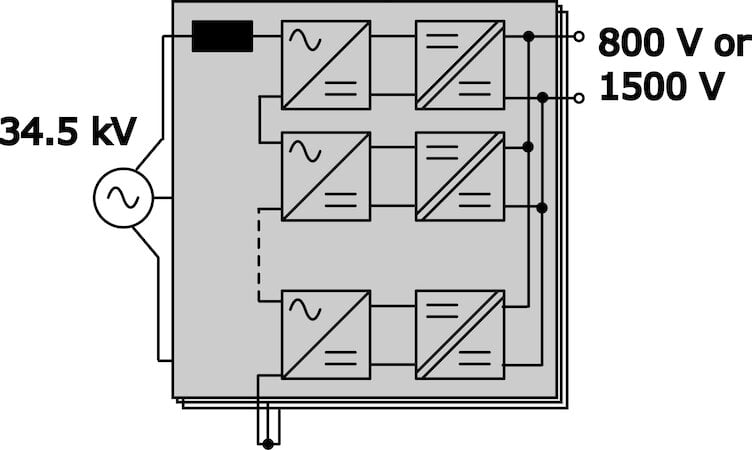
Figure 2. Simplified SST architecture with multiple cells being connected in series at their input. Image used courtesy of Bodo’s Power Systems [PDF]
Topologies and Solutions
Today, 800 V DC-bus systems are state-of-the-art for server-rack supply. However, motivated by the significant increase in power demand, higher system voltages like 1500 V are being discussed [9]. For PV inverters and battery-energy-storage systems, 1500 V is the widely accepted DC-voltage level as it represents the upper limit of the European Low Voltage Directive (IEC). In the following, both the 800 V and 1500 V use cases shall be analyzed in more detail.
The focus of the evaluation is limited to the isolated DC-to-DC conversion stage inside each cell of the SST. In this example, a dual-active bridge topology is considered as depicted in Figure 3. At the input side, which is connected via an AC/DC converter to the medium-voltage distribution network, 1800 V DC-link voltage is considered. Due to the comparably high operating voltage, grid voltages like 34.5 kV can be achieved with a reasonable number of cells, which limits system complexity.
In the following analysis, 16 cells are considered per phase.
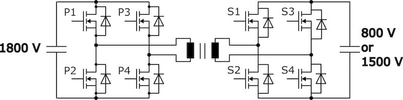
Figure 3. SST solution based on a Dual-Active-Bridge topology. Image used courtesy of Bodo’s Power Systems [PDF]
800 V DC-Voltage Output System
For the isolated DC/DC converter from 1800 V to 800 V, the considered Mitsubishi Electric SiC MOSFET power modules are, for the primary side, the FMF800DC-66BEW (3.3kV/800A) in the LV100 housing, and for the secondary side, the FMF600DXE-24BN (1.2kV/600A) in the NX housing with 2 devices in parallel. The operating conditions are listed in Table 1. The virtual junction temperature is estimated for the devices based on liquid cooling, with thermal resistances from the heatsink to the water of around 16K/kW and 30 K/kW for the LV100 and NX packages, respectively. The remaining parameters are taken from datasheets.
Table 1. Simulation conditions for a power supply system with a DC voltage output of 800 V.
| Switching frequency fC | 10 | kHz |
| Output power Pout | 550 | kW |
| DC input voltage Vin | 1800 | V |
| DC output voltage Vout | 800 | V |
| Turns ratio N | 2.25 | |
| Stray inductance Lσ | 25 | µH |
| Water temperature TW | 40 | °C |
| Primary side power module | FMF800DC-66BEW | |
| Secondary side power module | FMF600DXE-24BN | |
As shown in Figure 4, for the operating conditions in Table 1, the maximum virtual junction temperature of the primary-side and secondary-side power modules reaches 127 °C and 150 °C, respectively.
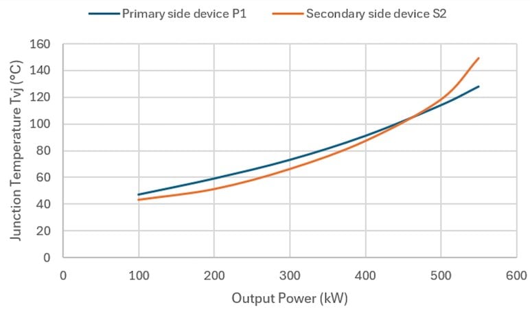
Figure 4. Simulation results showing maximum output power versus maximum junction temperature of the power module for DC-output = 800 V. Image used courtesy of Bodo’s Power Systems [PDF]
1500 V DC-Voltage Output System
For the isolated DC/DC converter from 1800V to 1500V, the considered Mitsubishi Electric SiC MOSFET power modules are, for the primary side, the 2 FMF800DC-66BEW in parallel, and for the secondary side, the 2 FMF1600DC-50CW (2.5 kV/1600 A) in parallel.
Both devices use the LV100 housing. Table 2 shows the operating conditions. The virtual junction temperature is estimated for the devices based on liquid cooling, with the thermal resistances from the heatsink to the water around 16 K/kW for the LV100 devices. The remaining parameters are taken from datasheets.
Table 2. Simulation conditions for a power supply system with 1500VDC output.
| Switching frequency fC | 10 | kHz |
| Output power Pout | 1.3 | MW |
| DC input voltage Vin | 1800 | V |
| DC output voltage Vout | 1500 | V |
| Turns ratio N | 1.2 | |
| Stray inductance Lσ | 5 | µH |
| Water temperature TW | 40 | °C |
| Primary side power module | FMF800DC-66BEW | |
| Secondary side power module | FMF1600DC-50CW | |
As shown in Figure 5, for the operating conditions in Table 2, the maximum virtual junction temperature of the primary-side and secondary-side power modules reaches 136 °C and 150 °C, respectively.
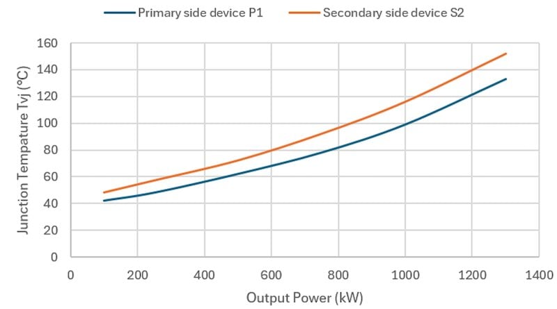
Figure 5. Simulation results showing maximum output power versus maximum junction temperature of the power module for DC-output = 1500 V. Image used courtesy of Bodo’s Power Systems [PDF]
The simulation results show that 550 kW and 1.3MW are realistic targets for an 800 V and 1500 V system. As stated above, for the connection to the 34.5kV distribution network, 16 cells are considered per phase, resulting in 48 cells for the three phases. Delivering 1.3MW per cell using Mitsubishi Electric SiC power modules results in a system output power of 62MW. It becomes evident that high-power SST and high-current SiC power modules are the crucial components for current data center power requirements of 50MW and higher. At the same time, they provide a scalable path to support future growth and improve “Tokens per Second per Megawatt”.
Power Modules Considered in This Analysis
The primary side requires power modules with 3.3kV SiC MOSFETs, while the secondary side power modules are either 1.2kV SiC MOSFETs for 800V output or 2.5 kV SiC MOSFETs for the 1500V output. Each power module is a half-bridge consisting of 2 switches in a package. While the 1.2kV power module is available in the NX housing, the 2.5kV and 3.3kV power modules are available in the LV100 housing.
1.2 kV SiC MOSFETs
Power module package compatibility is a key aspect that system designers need to consider when new solutions are being developed. Widely utilized conventional packages have been developed based on Si IGBT devices, and incorporating SiC devices in these conventional (but widely accepted) packages is challenging. SiC MOSFETs switch faster than Si IGBTs and require special power module design considerations with regard to internal current balancing of parallel-connected MOSFET dies and overall internal parasitic inductance.
The NX package is a widely adopted power module housing for several applications, including uninterruptible power supplies, photovoltaic, battery storage systems, and motor drives for output power in the range of several hundred kilowatts. A usual disadvantage of a conventional NX package is its high internal parasitic inductance in the range of 15 to 20 nH. The reason for this is the layout of the chips and the internal busbar design. High internal inductance presents a challenge for SiC adoption as it prevents the user from taking advantage of high switching speeds.
The Special NX Module for SiC Adoption
This problem was solved by introducing a special NX module (Figure 6) designed for SiC adoption [10]; its internal busbars are organized in a laminated structure (Figure 7). The SiC MOSFET dies were internally placed for optimum current sharing. The overall parasitic inductance of the NX SiC module is about 9 nH. The package utilizes an AlN ceramic substrate and offers 4 kV of isolation between the terminals and the baseplate.
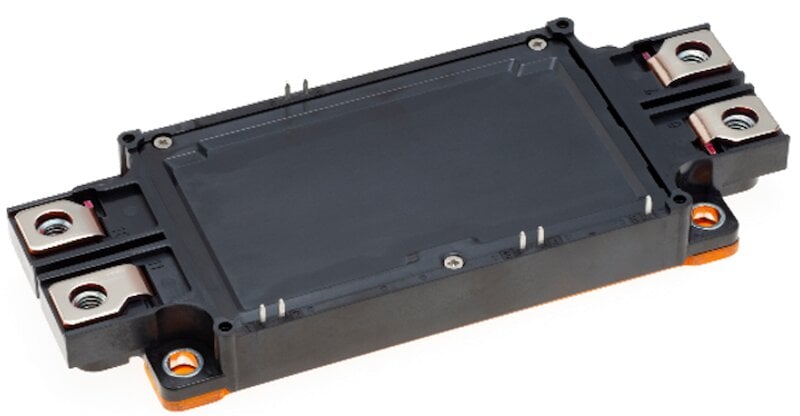
Figure 6. SiC MOSFET power module FMF600DXE-24BN in the NX package. Image used courtesy of Bodo’s Power Systems [PDF]
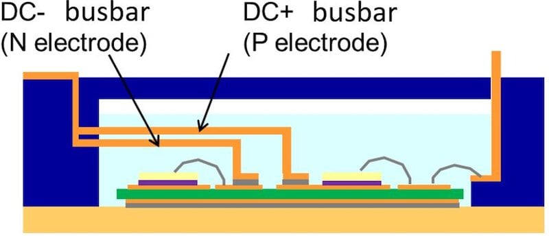
Figure 7. Cross-section of the NX SiC power module showing laminated busbar design. Image used courtesy of Bodo’s Power Systems [PDF]
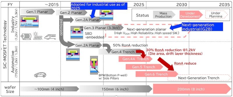
Figure 8. SiC Chip technology roadmap. Image used courtesy of Bodo’s Power Systems [PDF]
The NX SiC modules are currently available in the ratings of 1.7kV /600A (FMF600DXE-34BN) and 1.2kV/600A (FMF600DXE-24BN) and are provided with the second-generation Mitsubishi SiC chip technology. The low inductance package design allows the user to extract maximum performance from the advanced second-generation (G2A) SiC MOSFET chips.
The simulation results in Figure 4 indicate that the secondary-side device FMF600DXE-24BN is the thermal bottleneck. By utilizing power modules with lower RDS(on) and higher current rating, it is possible to extend the overall output of the power stage.
Referring to Table 3, the NX SiC power module line-up is being extended towards higher current ratings. Additionally, a new chip generation (G2B) is also under development to further optimize overall electrical performance (refer to Figure 8).
Table 3. Line-up of the 1.2 kV NX SiC power modules currently under development.
| Rating | RDS(on) [mΩ] at 150 °C | Status | Chip Technology |
| 1.2 kV / 600 A | 2.68 | Mass production | G2A SiC |
| 1.2 kV / 600 A | 2.4 | Under development | New G2B SiC |
| 1.2 kV / 800 A | 1.8 | ||
| 1.2 kV / 1000 A | 1.43 |
Reliability of SiC Power Modules
While power density and efficiency play a direct role in determining the revenue generation capability of the installed AI infrastructure, reliability and preventing downtime due to failures are often overlooked aspects in the overall cost-benefit calculation. There are several known degradation modes for SiC MOSFETs. The stability of the VGS(th) is one key aspect, and Mitsubishi SiC power modules have demonstrated good VGS(th) stability (refer to Figure 9). Another topic that is important for the long term is the so-called “bipolar current degradation” [11]. Referring to Figure 10, it can be understood that, for a 5% increase in VDS(on), the estimated probability at the module level is about 100ppm, indicating robustness towards bipolar current degradation.
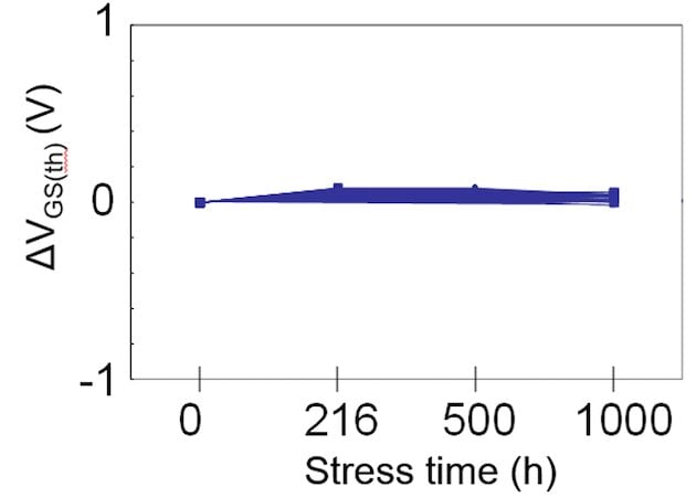
Figure 9. Delta VGS(th) vs stress time for Tvj = 150 °C, VGS = +20 V, duration = 1000 hours. N = 22 pcs. Image used courtesy of Bodo’s Power Systems [PDF]
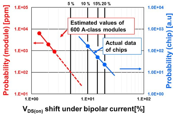
Figure 10. Probability of VDS(on) shift of SiC MOSFET chips due to bipolar current stress for a 1200 V SiC device. Image used courtesy of Bodo’s Power Systems [PDF]
2.5 kV and 3.3 kV SiC MOSFETs
Table 4 presents the line-up of the 2.5 kV and 3.3 kV SiC power modules which are applicable for the datacenter power supply application. The devices are available in the LV100 package (refer to Figure 11), which is accepted as the industry standard for high-power applications. The LV100 modules are widely adopted in megawatt-level PV and BESS applications, as well as traction applications. The LV100 package was developed considering SiC adoption for high-power applications and is therefore already optimized with regard to internal busbar layout and the internal chip placement. The LV100 module shown in Figure 11 utilizes an AlSiC baseplate for high thermal cycling capability and has an isolation voltage of 6kV between terminals and baseplate. Table 4 shows the line-up of the available SiC LV100 modules.
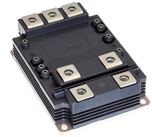
Figure 11. The LV100 package for the FMF1600DC-50CW and FMF800DC-66BEW. Image used courtesy of Bodo’s Power Systems [PDF]
The 2.5 kV / 1600 A SiC LV100 (FMF1600DC-50CW) has been specifically developed for PV and BESS applications requiring a 1.5 kV DC-link. For such applications, the best trade-off between cosmic ray FIT and electrical loss performance is required while maintaining sufficient margin for switching overvoltages, which is relevant when utilizing SiC high-switching-speed operation. Since the module utilizes the latest G2B SiC chip technology, it is optimized for best electrical loss performance (Qrr reduction using proton irradiation), and the module has a target FIT of less than 100 for 1500V.
Table 4. The line-up of the 2.5 kV and 3.3 kV SiC LV100 modules.
| Type Name | Blocking Voltage [V] | Rated Current [A] | RDS(on) at 150 °C [mΩ] |
| FMF1600DC-50CW | 2500 | 1600 | 1.75 |
| FMF200DC-66BE | 3300 | 200 | 17.25 |
| FMF400DC-66BEW | 3300 | 400 | 8.63 |
| FMF800DC-66BEW | 3300 | 800 | 4.31 |
3.3 kV SiC MOSFET
In 2024, Mitsubishi Electric released the Unifull™ SiC power modules with embedded Schottky Barrier Diode (SBD) [12][13]. The embedded SBD effectively solves the issue of bipolar degradation by deactivating the internal body diode of the SiC MOSFET. Furthermore, as the body diode is deactivated, Unifull SiC power modules have no reverse recovery losses and reduced turn-on losses. Exemplary switching waveforms shown in Figure 12 demonstrate the absence of recovery charge and the higher switching speed of the Unifull power modules. Overall, switching losses of Unifull 3.3kV SiC MOSFETs are reduced by 58 %, compared to the previous 3.3kV SiC generation, as shown in Figure 13.
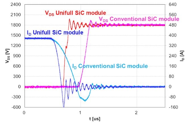
(a) diode reverse recovery
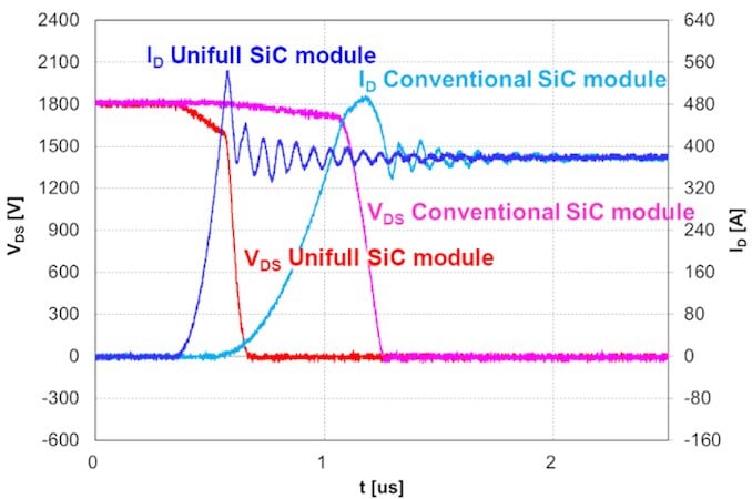
(b) MOSFET turn-on
Figure 12. Switching waveform comparison between conventional 3.3 kV SiC MOSFET (FMF375DC-66A) and Unifull™ 3.3 kV SiC MOSFET (FMF400DC-66BEW). Image used courtesy of Bodo’s Power Systems [PDF]
Mitsubishi Electric has specially developed Unifull 3.3 kV SiC power modules for high-reliability applications like railway traction and grid applications. 6 kV isolation voltage and partial-discharge-free design according to IEC 61287-1 make this device suitable for direct operation at the high-voltage electricity grid. In case of unforeseen events, surge current and I²t values are specified as 5.9 kA and 180kA²s, respectively.
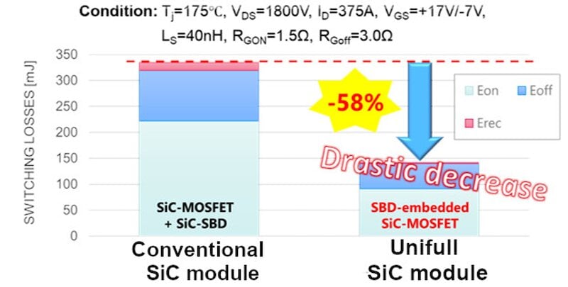
Figure 13. Switching loss reduction of Unifull™ 3.3 kV SiC MOSFET (FMF400DC-66BEW) compared to conventional 3.3 kV SiC MOSFET (FMF375DC-66A). Image used courtesy of Bodo’s Power Systems [PDF]
Unifull power modules use sintering to attach the SiC dies to the substrates. This increases the power-cycling capabilities compared to conventional soldering technology. To provide even higher power-cycling capability for especially demanding applications, Unifull™ Plus technology has been developed [14] recently. As visualized in Figure 14, enhanced bond-wire material and chip metallization are utilized for Unifull Plus. Measurements confirm that Al-alloy wire and enhanced metallization achieve approximately 5 times higher power-cycling capabilities than the original Unifull bond-wire material (refer to Figure 15).
High efficiency, fast switching speed, and high ruggedness make Unifull Plus power modules especially suitable for SSTs with direct grid connection.
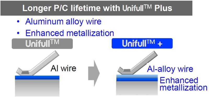
Figure 14. Unifull™ Plus uses enhanced bond wire and chip metallization to increase power-cycling capabilities. Image used courtesy of Bodo’s Power Systems [PDF]
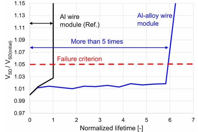
Figure 15. Al-alloy wire and chip metallization, as used in Unifull™ Plus technology, allow 5 times longer power-cycling lifetimes. Image used courtesy of Bodo’s Power Systems [PDF]
Conclusion
AI-driven datacenters require power-supply solutions that combine high efficiency, power density, scalability, and reliability. SST architectures based on SiC power modules can achieve these requirements, while allowing direct conversion from the medium-voltage distribution network to 800V and future 1500V DC datacenter infrastructures while supporting these requirements.
The analysis shows that 550 kW and 1.3 MW are realistic targets for 800V and 1500V SST cells, respectively. For a 34.5kV distribution network considered in this work, the resulting SST can achieve more than 60MW of power capability. High-power SSTs utilizing high-current SiC power modules therefore represent a scalable solution for current and future hyperscale data centers while improving the key AI efficiency metric: “Tokens per Second per Megawatt.”
References:
[1] IEA (2025), Energy and AI, IEA, Paris https://www.iea.org/reports/energy-and-ai, License: CC BY 4.0
[2] AI power: Expanding data center capacity to meet growing demand, McKinsey & Company. March 25, 2026.
[3] Bloom Energy, 2026 Data Center Power Report: When Power Defines Growth: How Power Availability Is Reshaping the Data Center Industry, Bloom Energy, Jan. 2026. [Online]. Available: https://www.bloomenergy.com/wp-content/ uploads/2026-power-report.pdf. Accessed: Jul. 30, 2026
[4] Siemens, Report “DATA CENTERS 100 MW Hyperscale AI Blueprint”, URL: https://assets.new.siemens.com/siemens/assets/api/uuid:ccfd2c1e-4e8b-423c-bec3-17333e651cde/DataCenter-Reference-Architectures-100MW-Blueprint_original.pdf
[5] Deloitte, Article “AI data centers jolt power demand”, ULR: https://action.deloitte.com/insight/4718/ai-data-centers-joltpower-demand
[6] Scaling Token Factory Revenue and AI Efficiency by Maximizing Performance per Watt, NVIDIA. URL: https://developer.nvidia.com/blog/scaling-token-factory-revenue-and-ai-efficiency-by-maximizing-performanceper-watt/
[7] Predescu, D.-M.; Roșu, Ș.-G. Solid State Transformers: A Review—Part I: Stages of Conversion and Topologies. Technologies 2025, 13, 74. https://doi.org/10.3390/technologies13020074
[8] J. Huber and J. W. Kolar, “Next-Generation Solid-State Transformers for Powering Artificial Intelligence Data Centers: A Survey of Emerging Topologies,” in IEEE Industrial Electronics Magazine, vol. 20, no. 2, pp. 42-54, June 2026, doi: 10.1109/ MIE.2026.3684540.
[9] Open Compute Project, Report “Data Center Facility – Low Voltage Direct Current Power Distribution”, 30 March, 2026. URL: https://www.opencompute.org/documents/dcf-powerdistribution-lvdc-white-paper-version-1-0-final-pdf-1
[10] R. Goto, Y. Miyazaki, N. Lakshmanan, K. Masuda and E. Motto, “Advanced PKG technology for SiC in the NX Package,” PCIM Europe 2023; International Exhibition and Conference for Power Electronics, Intelligent Motion, Renewable Energy and Energy Management, Nuremberg, Germany, 2023, pp. 1-6, doi: 10.30420/566091120.
[11] K. Ishibashi et al., “Prediction of the Bipolar Degradation in 1200V 4H-SiC MOSFETs by Inspection in Device Fabrication Process,” PCIM Europe 2023; International Exhibition and Conference for Power Electronics, Intelligent Motion, Renewable Energy and Energy Management, Nuremberg, Germany, 2023, pp. 1-5, doi: 10.30420/566091021.
[12] N. Soltau, D. He, R. Tsuda, and S. Yamamoto, “How a Unifull SiC Power Module Reduces Carbon Emissions in the Transportation Sector,” Bodo’s Power Systems, September 2024, pp. 16-21
[13] Y. Hironaka, S. Okimoto, M. Matsuo, S. Saito, K. Hatori and N. Soltau, “3.3 kV SBD-Embedded SiC-MOSFET Module for Traction Use,” PCIM Europe, Nuremberg, Germany, 2024, pp. 699-706
[14] D. Yosho et al., “Investigation of Power Cycling Lifetime: Extension from Si to SiC and Enhancement of SiC Module Lifetime by Advanced Materials,” 2025 Energy Conversion Congress & Expo Europe (ECCE Europe), Birmingham, United Kingdom, 2025
This article originally appeared in Bodo’s Power Systems [PDF] magazine and is co-authored by Narender Lakshmanan, Karthik Debbadi, and Nils Soltau, Mitsubishi Electric Europe B.V. (based in Ratingen, Germany), and Ryo Tsuda, Mitsubishi Electric Power Devices (based in Fukuoka, Japan)