Facebook
 Google
 GitHub
 Linkedin
High-Voltage Isolated Gate Driver Module
This article features the IXYS' IXIDM1401 high-voltage isolated gate driver module and its features, higher performance and reliability.
IXYS 4000V MOSFET and IGBT Driver Module Provides Supreme Compactness with the Highest Performance and Reliability. The Goal is to Serve Motor Drives, Inverters, Converters, Medical, UPS, Traction and Industrial Switched-Mode Power Supply (SMPS) products that enable the shortest design cycle as well as the lowest design cost.
Introduction
The IXIDM1401 is a high-voltage isolated gate driver module based on the IX6610/IX6611 chipset, which allows creation of an isolated IGBT driver with a high voltage isolation barrier between the primary and secondary sides as well as between secondary side drivers. This creates a very flexible architecture, which can be used for 3-phase motor drivers, half-bridge switches, push-pull converters, or other applications in UPS, renewable energy, and transportation, which require isolation between primary and secondary side and/or between secondary side drivers.
An internal power supply provides up to 2 W per channel of isolated power to drive both upper and lower IGBTs, effectively isolating the MCU from the high power circuitry. Operating from a single polarity 15 V power source, it provides +20 V/-5 V to drive the IGBT gates and +3.3 V to drive the MCU, maintaining up to 4 kV isolation voltage between the MCU and gate drivers and between gate drivers as well.
Over and Under Voltage Protection
Built-in under-voltage and over-voltage protection prevents the IGBTs from operating at gate voltages outside of the optimal window and informs the MCU about such conditions without regard to the source of the problems, which may come from either the low/high side IGBT behind the isolation barrier or the primary side before the isolation barrier.
Over-Current Protection
An over-current protection with a 300 mV threshold can be implemented by utilizing either a current-sense resistor or IGBT de-saturation event. It turns the IGBT off immediately after the collector current exceeds a value set by the user and informs the MCU to make an appropriate decision.
An Active Clamping Comparator with a 3.1 V threshold (with respect to the negative IGBT gate voltage) disables the driver when the collector voltage exceeds the level set by the user, preventing excessive power dissipation in the IGBTs.
Asynchronous Data Transmission
TTL level compatible input signals from an external MCU are used to operate secondary-side drivers. The IXIDM1401 implements a dual-channel bidirectional transformer interface, which transmits the primary side input commands from the MCU to the secondary side and information from the secondary side to the MCU. Asynchronous data transmission is implemented by narrow pulses to prevent the transformer’s core saturation.
A narrow pulse detector is also implemented to prevent transmission of very narrow false PWM input signals to the drivers. Input signal pulses with width narrower than 100 ns are suppressed and pulses with width greater than 350 ns are transferred to the drivers.
To avoid limitations to the input pulse maximum width, only short pulses representing rising/falling edges of the input signals are transmitted from the primary side, while the secondary side restores the original pulse width.
The secondary side gate drivers convert the incoming PWM logic signals into +20 V/-5 V (in respect to COMMON) bipolar gate drive signal with a typical 10 A peak drive current capability. Separate positive and negative gate driver outputs allow optimization of IGBT turn on/off time without an external diode by selecting serial gate resistors of different values.
Dead Time Delay
The built-in dead time delay circuitry, with channel A priority, prevents the IGBTs from turning on simultaneously. If channel B is active and channel A is forced into on-state, channel B becomes disabled immediately and the channel A IGBT turns on with a preset delay time. After channel A becomes inactive, channel B, if active, turns on with the same delay time. If channel A is active and channel B is forced into on-state, this command will be ignored as long as channel A remains active. If channel A becomes inactive before the command activating channel B expires, channel B becomes active with a preset delay time after channel A becomes inactive.
It allows using a single input signal source to create a complementary switching pair of IGBTs in a half-bridge configuration by setting channel B to permanently enabled and operating channel A only.
Dead time between pulses at Gate A and Gate B outputs is hardware programmed to ~420 ns. If the dead time required to operate specific IGBTs is greater than implemented in IXIDM1401, it should be programmed by the MCU or factory-adjusted to the required value.
Over-Temperature Protection
The over-temperature protection function disables the IGBTs if the internal chip’s temperature exceeds 1500 C, and resumes normal operations when the temperature falls below 1250 C. If the IGBT assembly is equipped with a temperature sensor, the IXIDM1401 is able to translate its signal to the MCU.
A dual-channel bidirectional transformer interface allows transmission of information to the MCU about secondary side power supply faults and IGBT over-current conditions.
Fault Signals
All fault conditions at the primary side stop execution of the PWM cycle at both drivers, while all fault conditions at the secondary side stop the PWM cycle at the affected driver only. If fault conditions appear before the start of the PWM cycle, the PWM cycle will be ignored as long as fault conditions exist.
The IXIDM1401 power block is designed to provide up to 2 W of power. It has a start-up mode and a run mode. In the start-up mode, the converter operates from the internal oscillator and activates only a portion of the power switches to reduce the dynamic current consumption/power dissipation. After start-up, the converter activates the entire power switches and goes into run mode. The run mode is held off ~1.28 ms. Transmit operation is disabled during start-up mode to minimize current draw in the secondary. After run mode begins, it will continue until a restart occurs, which returns the power block to start-up mode.
In the run mode, the power block operates either from an internal or external clock. Use of an external clock from the MCU enables minimizing noise interference between IXIDM1401 devices in case of multi-phase applications like motor drivers.
The power block’s push-pull converter duty cycle depends on the external clock duty cycle as DCPL = 0.5 – DCEXT/2.015 that allows for adjustment of secondary output voltage by varying the duty cycle in case of over/under-voltage.
A converter’s watchdog timer prevents potential damage due to the absence of an external clock. Whenever the external clock period exceeds the watchdog timeout of 40 µs, the converter switches to the internal clock.
Active Clamping Protection
Active Clamping protection implemented in IXIDM1401 enables prevention of IGBT damage in case of an inductive load turned off with high inductive current. In such situations, the IGBT collector voltage may easily exceed the breakdown limit and destroy the IGBT. One of the ways to prevent this condition is to keep the IGBT conducting until the energy stored in the inductor is not enough to create a collector over-voltage condition. The IXIDM1401 utilizes ACL comparators with 3.1 V thresholds in respect to negative voltage source that may be used for implementing an advanced active clamping technique.
Triggering the ACL comparator forces the gate driver output to a tri-state condition and the IGBT starts to turn on due to the breakdown diode current charging the IGBT gate. After the IGBT turns on, its collector voltage falls, the diode recovers from breakdown, and the ACL comparator turns on the OUTN output, which forces the IGBT gate low. This sequence may repeat several times until the energy in the external inductance is dissipated. The ACL comparator is active only when the driver’s output OUTP is OFF.
Each of the IXIDM1401 IGBT drivers also contains an over-current (OC) comparator with a 300 mV threshold in respect to the COMMON pin. Over-current protection can be implemented either by using a low-value current sense resistor, an IGBT with a secondary current sense output, or utilizing a de-saturation event.
If an over-current fault occurs, the driver’s output is forced low for the rest of the cycle. Normal operation resumes at the beginning of the next PWM gate drive cycle.
A noise filter at the current sense input may be required due to low sense voltage. The OC comparator has an internal 100 pF capacitor connected in parallel to the input; therefore, only a serial resistor can be added to create such a filter. The OC comparator’s input is grounded during the off-time of the IGBT and remains grounded for 3.5 µs immediately after the IGBT turns on to prevent false tripping. When an over-current event occurs, the Output Faults Pulse Generator creates a narrow 200 ns pulse that is used by the Fault Control Logic to communicate the fault condition to the MCU.
The IXIDM1401 is available in a 50 x 50 x 25 mm package with a 12-pin, 1 mm-pitch FFC connector to communicate with an MCU, two 5-pin, 2.54 mm-pitch headers to provide signals to/from the IGBTs, and one 2 pin, 2.54 mm-pitch header to translate signals from an external temperature sensor to the MCU.
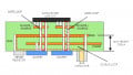
One of the possible applications, shown in Figure 1, represents IXIDM1401, which operates IXYS Corporation’s phase leg IGBT module MIXA225PF1200TSF.

Figure 1: IXIDM1401/ MIXA225PF1200TSF Modules Assembly
Power Supply
Powered from a single polarity 15 V power supply, IXIDM1401 operates two 1200 V IGBT devices with a maximum collector current of 360 A. This design allows the MCU to alert customers about under/over-voltage conditions on the primary and secondary sides, and overload conditions when the IGBT goes into de-saturation mode. The MCU can be powered from this module and does not require a separate power source. If a user prefers to drive the MCU from an external power source, this can be accomplished as well. Internal IXIDM1401 logic can be also powered from the same external source, minimizing power consumption from the 15 V power supply.
Typical applications for this design are shown in Figures 2 and 3.

Figure 2: Typical Application Circuit of a Three-phase Motor Driver

Figure 3: Typical Application Circuit of a Full-bridge Inverter
Figures 4 – 7 display IXIDM1401 performance with the 10 nF gate load capacitance, while figures 8 – 13 display IXIDM1401 performance with MIXA225PF1200TSF module as a load. In each of the figures below, the yellow curve represents an input signal, while the green and magenta curves represent output signals.

Figure 4: Input to Output Propagation Delay Channel: A Rising Edge (10 nF load)

Figure 5: Input to Output Propagation Delay: Channel B Rising Edge (10 nF load)

Figure 6: Input to Output Propagation Delay: Channel A Falling Edge (10 nF load)

Figure 7: Input to Output Propagation Dela:y Channel B Falling Edge (10 nF load)

Figure 8: Input to Output Propagation Delay Channel A Rising Edge (MIXA225PF1200TSF load)

Figure 9: Input to Output Propagation Delay Channel B Rising Edge (MIXA225PF1200TSF load)

Figure 10: Input to Output Propagation Delay Channel A Falling Edge (MIXA225PF1200TSF load)

Figure 11: Input to Output Propagation Delay Channel B Falling Edge (MIXA225PF1200TSF load

Figure 12: MIXA225PF1200TSF operating in complimentary mode with a single signal source at channel A and channel B permanently enabled

Figure 13: Dead time generated by IXIDM1401 in complementary mode
About the Authors
Abdus Sattar works as the Director of Engineering at IXYS Corporation. He is responsible for leading the vision to drive product roadmap, product planning, new product development, and solve complex customer issues with strategic tradeoffs between cost, features, and performance; align priorities with corporate objectives while optimizing resources by balancing large-scale projects with cross-functional resources to meet deadlines; and act as a strategic innovation leader to CEO and CTO and deployed product line strategy to bring new ideas for evaluation and potential rollout and implementation. He is a graduate of a Bachelor's and Master's degree in Electrical Engineering at Rajshahi University of Engineering & Technology and South Dakota State University respectively. He then earned his PhD in Electrical Engineering at Santa Clara University, California, USA.
Leonid Neyman works as the Senior Applications Manager at IXYS Corporation, a company that focuses on the manufacture and development of power semiconductors, radio-frequency (RF) power semiconductors, and digital and analog integrated circuits.
This article originally appeared in the Bodo’s Power Systems magazine.