Facebook
 Google
 GitHub
 Linkedin
High Power Electronics Cleaning Requirements for Improved Efficiency and Reliability
This article highlights the importance and benefits of cleaning power modules before bonding to ensure long-term reliability.
Today, power modules are widely used in high power applications such as hybrid electric vehicles, solar inverters, medical equipment, and UPS (Uninterruptable Power Supplies) devices. For energy efficiency reasons, high power devices such as MOSFETs, IGBTs and DCBs are subjected to increased performance requirements with greater packaging density and involves various metal material mix.
Moreover, the oftentimes are subjected to elevated temperature and power cycling environments, extremely high current flow and extreme thermal transfer requirements. Accordingly, even the slightest contaminants remaining on the surface will impede the reliability required in these critical and highly sensitive applications.
During the power module manufacturing process, contaminants including oxide films and flux splatter remain on the substrate and chip surfaces. In order to guarantee the highest process reliability, these contaminants must be completely removed from the surfaces through a cleaning process.
There are several process flows for power module production and thus various process steps that require cleaning. Although the production process may vary based on the application, design and functionality of the power devices, typically cleaning is required following die attach to copper substrate prior to wire bonding and after heat sink soldering prior to further processing such as bonding and molding.
This paper, originally presented in Bodo’s Power Systems, details power module applications including typical qualification tests, failure mechanisms and considerations for cleaning processes [1]. Subsequent to its release, engineered aqueous-based cleaning agents have been incorporated into power module manufacturing processes. Several customer case studies highlighting this cleaning alternative and the reliability impact on the process are detailed within this paper.
Background
There are several process flows for power module production and thus different stations, where cleaning is usually required. The production process flow may differ due to the field of application, such as for automobile and industrial operation, as well as due to the design and functionality as defined by the end customer.
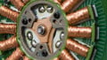
Usually, the first production step is the die attach to the copper substrate by soldering, for example of IGBTs and diodes (Figure 1). Afterwards, production flows may vary. In any case, there are two points where cleaning is highly recommended. The first point would be after die attach by soldering to prepare the modules for wire bonding and the second would be after heat sink soldering before the modules are further processed, for example, molded, wire bonded and/or connected to frames.

Figure 1: Cleaning Applications in Power Module Production
Irrespective from the process flow and final module structure, contaminants such as oxide films and flux spatter remain on the chip and substrate surface after soldering. These residues have a negative impact on subsequent processes such as wire bonding or molding. Wire bond adhesion is often impaired when flux splatter remains on surfaces. Residues on the substrate and chip surfaces can impair achievable shear values for copper, diodes and IGBTs. Since these values are often used for the cleanliness qualification, it is necessary to completely remove all residues in a suitable cleaning process.
Qualification Procedure
Typically, extensive qualification testing is performed to determine the reliability of power modules. This enables manufacturers to qualify products in accordance with internationally accepted tests. Examples of standard qualification tests based on IEC and CENELEC standards are detailed in Table 1.
|
Environmental Assessment |
||||
Qualification Test |
Test Method |
Test Conditions |
Qualification Standard |
|
Thermal Shock |
IEC68-2-14 |
-40°C to + 125°C2 hrs at each extremeTransfer Time = 30s |
100 cycles |
|
Mechanical Shock |
IEC68-2-27 |
20g/20msec/half sine |
30 shocks10 in each of 3 axes |
|
Humidity |
IEC60749-5 |
Tj = 85°CRH = 85%Vce = 80VVge = 0V |
1000 hours |
|
Vibration |
IEC68-2-6 |
F = 55 to 500HzAcceleration = 10g |
6 hours2 hrs in each of 3 mutually axes |
|
Electrical Assessment |
||||
Power Cycling |
CENELEC |
∆Tj = 50°CCycle Time = 2-5 secs |
1M cycles |
|
Low Temp Storage |
IEC68-2-1 |
Ta = -40°C |
1000 hours |
|
High Temp Storage |
IEC68-2-2 |
Ta = 125°C |
1000 hours |
|
Moisture Resistance |
IEC68-2-3 |
Ta = 60°C, RH = 90% |
1000 hours |
|
HTRB |
-- |
Ta = 125°CVce= 0.8V * Vce (max)Vge = 0V |
1000 hours |
|
HTGB |
-- |
Ta = 125°CVce = 20V |
1000 hours |
|
Intermittent Operation |
-- |
∆Tc = 50°C(∆Tj = 100°C) |
5000 cycles |
|
Table 1: Standard Qualification Tests Based on IEC and CENELEC Standards
Advantages of an Optimized Cleaning Process
Although solvents were traditionally used to clean power electronics, aqueous-based cleaning processes have become the norm over the past few years. Aqueous-based cleaning agents specifically developed for power electronics provide excellent cleaning performance while ensuring material compatibility and long-term reliability of the power modules at the same time. They offer additional benefits such as significantly lower VOCs (Volatile Organic Compounds) and greatly improve health and safety.
Field data has confirmed that an optimized aqueous-based cleaning process offers numerous advantages with regard to wire-bond quality and reliability, as determined through shear tests and power cycling as well as molding and material compatibility.
Wire Bonding Quality – Shear Tests
There are two main issues that influence wire bond quality. These are flux residues on the substrate after soldering and more importantly, flux spatter remaining on the chip surfaces (Figure 2).


Figure 2: Diode uncleaned (Top) and cleaned (Bottom)
Bonding on uncleaned chips leads to insufficient quality and often results in either unnecessary high bonding power which leads to heel cracks, chip defects, or lift-offs due to poor wire connection. Reference Figures 3-5.

Figure 3: Heel cracks

Figure 4: Chip defect

Figure 5: Bond lift off
Ideally, power modules require visually flawless and spot-free substrates and chip surfaces. However, the soldering process or unsuitable cleaning agents, amongst other things, can lead to heavily oxidized parts. These oxide layers on the surface can lead to problems during bonding and can impair the production yield (Figure 6).

Figure 6A: Bonds on heavily oxidized Cu substrate

Figure 6B: Bond on Cu substrate activated by cleaning
A suitable cleaning process must achieve excellent cleaning performance in order to remove all flux residues from soldering and be able to activate oxidized surfaces. With a cleaning process optimized for power devices, the surfaces are optimally prepared for bonding. Field data has demonstrated that aqueous-based, pH neutral cleaning media can achieve these results as compared to traditionally flammable solvents thereby producing excellent bond yields and visually flawless parts.
The quality of the wire bonds is usually evaluated by shear testing. A stable process with high shear values and low standard deviation is required for production yield as indicated by Figure 7, referencing an ideal cleaner. Modules failing to pass shear tests can negatively impact process efficiency and costs, especially if the substrates are already soldered to the heat sink.

Figure 7: Shear value comparisons: Ideal cleaner
In conjunction with customer projects, Zestron investigated the effect cleaning had on shear values as part of an internal study [2]. Wire bond yield comparisons were made on substrates that were not cleaned and cleaned with a micro phase cleaner. Results proved that micro phase cleaning agents greatly increase shear values as compared to those achieved with uncleaned power modules (Figure 8).

Figure 8A: Shear value comparisons: Uncleaned power module

Figure 8B: Shear value comparisons: Modules cleaned before bonding
Given an optimized aqueous-based cleaning process, even plasma treatment, which has been typically necessary, can be eliminated thereby leading to significant cost reduction potential.
Long-term Reliability – Power Cycling Results
The aim of cleaning is always to guarantee long-term reliability of the power modules. The widely used method to qualify the long-term reliability or lifetime is power cycling. Typical qualification test methods include: thermal shock, mechanical shock, humidity, vibration, low and high temp storage, moisture resistance, HTRB, HTGB and intermittent operations. The modules are stressed based on specific life cycle models of their dedicated application with their lifetime typically measured in cycles.
If the modules have not been sufficiently cleaned and contaminants still remain on the chip and substrate surfaces, they oftentimes will fail power cycling tests. The most common failure are bond lift-offs caused by poor bond connections due to residues. Once a bond connection fails, the stress on the others is raised, usually leading to an exponential increase in the number of bond failures finally resulting in the breakdown of the power module.
Cleaning the modules prior to bonding has a significant impact on the power cycling results. If the residues from soldering are removed completely through an optimized process, the bond quality is thereby improved, long-term reliability is increased yielding excellent power cycling results. In comparison, modules cleaned in a conventional process statistically show shorter lifetimes.
Molding Adhesion
The cleaning process also impacts molding quality. In many cases, molding is applied to the bonded substrates to protect
them from environmental influences. Contaminants play a decisive role with regard to molding adhesion and thus reliability. Flux residues on the substrate surface reduce molding adhesion forces, which in turn may lead to delamination. Reference Figures 9-10.

Figure 9: Delamination

Figure 10: Delamination
They may also lead to electrochemical migration beneath the molding resulting in-field failures. In the course of several cleaning projects, it was proven that cleaning increases the adhesion forces while limiting delamination defects and thereby improves the molding reliability.
Material Compatibility
When seeking a cleaning process for high power devices, the cleaning performance is usually the main point of interest with regard to bonding and production yield. However, another important aspect is often neglect ted, that is the compatibility of the cleaning process with power module materials.
Cleaning agents for power modules must meet exceptional material compatibility requirements. Thus, the cleaning agent selection is critical to ensure it does not affect various chip passivations or the substrate surface itself. Unsuitable cleaning agents attack the passivation layers thus leading to the impairment of the chip function. The adverse effect of a cleaning agent on glass passivation of a thyristor is represented in Figure 11.

Figure 11A: Attack by an unsuitable cleaning agent

Figure 11B: Optimally cleaned using suitable cleaning agent
Additional material compatibility issues that could possibly arise are detailed in Figure 12 and Table 2.

Figure 12: Material compatibility issues
Area |
Metal Material Mix |
Possible Issues |
A |
Nickel Substrate |
Discoloration |
B |
Bath Copper |
Oxidation |
C |
Solder Side |
Oxidation |
D |
Insulated Material |
Destroy |
E |
Aluminum Die |
Oxidation |
Table 2: Material Compatibility Issues
It is therefore recommended to test not only the cleaning performance of the cleaning agent, but also to ensure that it is fully compatible with different metal material subsets before a process is implemented.
Summary
Cleaning power modules before bonding is a must to ensure their long-term reliability. Adjusted processes with cleaning agents specifically developed for power modules ensure highest cleanliness levels and thus increase bond and mould quality. At the same time, they ensure compatibility with chip passivations and substrate materials. Significantly improved results of the shear test and power cycling qualification finally lead to an increase in production yield. ZESTRON has already implemented several high volume processes in this area for automotive and industrial applications and is ready to support you with the selection or optimization of your power electronics cleaning application.
About the Authors
Thomas Kucharek has been working in the Application Technology department of ZESTRON Europe since 2002. He is the Deputy Head of Application Technology and is responsible for the technical assistant technical team of application engineering and supports the engineering team in developing and implementing specific cleaning processes for worldwide customers.
Ravi Parthasarathy works as the Senior Application Engineer at ZESTRON Americas, Manassas, Virginia. He earned his Bachelor's Degree in Chemical Engineering at University of Mumbai, Maharashtra, India. He then proceeded to Master's Degree in Chemical and Natural Gas Engineering at Texas A&M University, USA.
Jigar Patel is one of the Senior Application Engineer at ZESTRON Americas, Manassas, Virginia, a company that provides high precision cleaning products, services and training solutions for the electronics and semiconductor manufacturing industries. He earned his Master's Degree in Chemical Engineering at Wayne State University, Detroit, Michigan, USA.
References
- Thomas Kucharek, ZESTRON, “Cleaning of Power Module Substrates” Bodo’s Power Systems, May 2012.
- Stefan Strixner, ZESTRON, “Wire Bonding Process” EPP Europe, June 2007.
- Acceptability of Electronic Assemblies, IPC-A-610F