Facebook
 Google
 GitHub
 Linkedin
Numerical Modeling in Design for Reliability of Power Modules
This article sums up relevant failure modes as well as their causes and explains how numerical modelling can support design processes of development.
This article deals with today’s reliability issues of power modules. It sums up relevant failure modes as well as their causes and explains how numerical modelling can support design processes in different phases of development. As an example, a lifetime modelling technique for aluminum thick bond wires in power modules is described in more detail.
Power electronics remains a fast-growing field and also a changing one. Amongst the main driving business sectors for trends in power electronics are power generation and the automotive industry. New applications demand higher power and power densities as well as higher efficiency and miniaturization. Also, the places of installation accumulate and bring with them harsher environmental conditions. For example, mounting places close to the engine in hybrid cars experience high temperatures combined with vibrational loads and offer few space. To fulfill the growing demands, the use of new assembly and packaging technologies as well as new materials are necessary. Thus a need for expertise in reliability arises when designing and manufacturing power modules.
The reliability of power electronics can be addressed and improved already in early design phases by modelling techniques. In that way, the effort for prototyping and testing can be reduced and the whole design process can be improved and shortened. In order to be able to correlate package design with reliability measures, an understanding needs to be based on the underlying physical and chemical relation-ships as far as it is useful for solving the design question. This article gives an example on the package-oriented Physics of Failure (PoF) approach.
The main failure modes for classical interconnects in power electronics are bond wire lift-off, bond wire heel crack, die attach degradation, DBC delamination and DBC attach degradation. Figure 1 gives an overview.

Figure 1: Failure modes in a power electronic module
They are caused by the difference of the coefficients of thermal expansion (CTE) of the adjoining materials. When a power electronic chip is heated up, the different components expand at different ratios. This leads to mechanical stresses within interconnections and interfaces.
A silicon chip has a CTE of about 2.5 ppm/K, copper of about
17 ppm/K. When heated up (or cooled down) this leads to mechanical tension in the solder or sintering layer. If repeated temperature swings are applied, a crack will be initiated and continue to grow until the thermal path is degraded. As a result, the chip will eventually overheat and fail.
An aluminum bond wire has a CTE of about 23 ppm/K. Due to the local mismatch to the CTE of the semiconductor, temperature cycles will lead to degradation of the interface with crack growth and finally bond wire lift-off. The relative movement of the two bond sites of a wire bond caused by bending of the substrate (global CTE mismatch) exerts stresses on the bond wire, which can cause heel cracks. DBC delamination results from the mechanical tension in the bonding interface between ceramics. It is also driven by the differences in CTE of both adjoining materials and strongly depends on the amplitude of the temperature swing.
A newly developed method to calculate the lifetime of wire bonds subjected to active power cycling will now be explained in more detail. The failure mode addressed is the propagation of cracks in the interface or close to the interface of wire bond and chip. As mentioned above, it is caused mainly by the local CTE mismatch between the chip and wire material. This interface crack is roughly oval or circular and reduces the effective bond area until finally the bond lifts off from the substrate. The method has been applied to aluminum thick wire bonds of 300 µm and 400 µm thickness that are commonly used in power modules.
Amongst Physics-of-Failure models, the most commonly used model for fatigue of metals is the Coffin-Manson approach.
`N_f=C_1*(Δε_(p1))`
Thus, a lifetime Nf for a specific load scenario can be predicted from a damage parameter Δε, which can be obtained from numerical simulations. Alternatively to Coffin-Manson, a modified Paris approach can be used to calculate not only the time to failure, but the actual current crack area at any time:
`(dA)/(dN)=C_1*(Δε_(p1))^(C_2)`
Herein, dA/dN describes the increase of crack area per load cycle. This gives a couple of advantages:
- The crack growth parameters are not strictly limited to a single geometry, so the effect of different bond tools or bond parameters on lifetime resulting in different initial interface areas or different wedge geometries can be investigated.
- The decrease of thermal and electrical performance due to the deterioration of the interface can be considered as well as the interaction with other failure mechanisms.
- Crack growth is determined gradually so that no assumptions like miners rule are necessary to consider damage accumulation for complex load conditions
- Different failure criteria can be defined: As an example, the effect of the potting material properties on lifetime can be investigated. When the interface is sufficiently deteriorated, the bond will be lifted off the chip by the expansion of the potting when applying a thermal load.
To calibrate a crack growth model for Al thick wire bonds, Fraunhofer IZM has performed active power cycling tests to compile the necessary experimental data. Therefore, a special test setup was developed, that allows to performing active power cycling at defined temperature swings. The test stand comprises MOSFETs in linear operation mode at currents of 5-7 A sintered on DBC. For each bond that has been tested, the temperature swing was known and the crack propagation during cycling was monitored by shear tests and optic evaluation of the shear sockets. In this way 300 µm and 400 µm wires have been tested at the temperature swings 75 K, 85 K, 95 K and 105 K (cooler reference temperature was 20 °C for all cases).
To obtain the damage parameter for the crack propagation equation, a numerical simulation model has been set up. It consists of a wire bond wedge, chip and chip metallization. The crack is included with parametrical size, so that the damage parameter can easily be calculated for different crack states. As damage parameter the plastic strains Δεpl accumulated from one cycle to the next are considered and averaged in an area near the crack front. An example strain distribution can be seen in Figure 2.
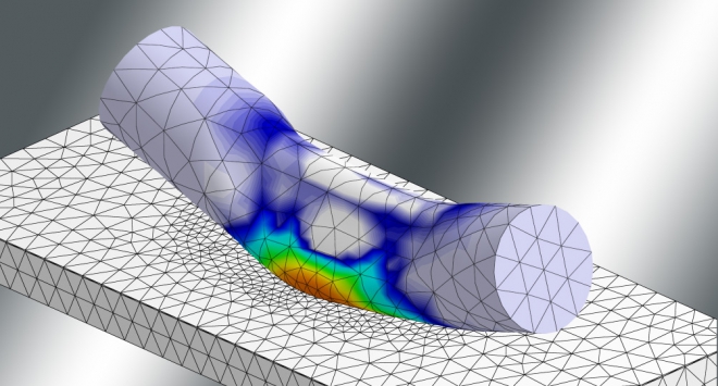
Figure 2: Finite element simulation submodel of wire bond wedge on semiconductor. The colors depict the strain distribution due to active power cycling.
The simulation results are sensitive to the material data used. Whereas silicon is well known and defined, the aluminum properties change with the wire material and microstructure of the bond and thus have to be characterized individually – by tensile tests or nanoindentation. Figure 3 shows the temperature-dependent stress-strain curves of an Al-H11 wire.
With the experimental power cycling data and the damage parameters calculated by the simulation models, a crack propagation law in the form of a modified Paris approach has been calibrated. This kind of model enables to predict crack propagation after any number of cycles for different load conditions. An example is given in Figure 4. There, failure is assumed when the remaining interface becomes smaller than the cross-sectional area of the wire.
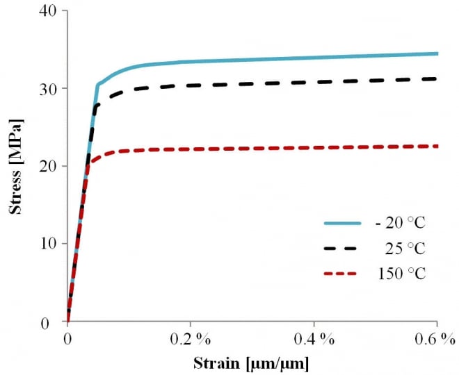
Figure 3: Temperature-dependent stress-strain curves of Al-H11 wire obtained from tensile test

Figure 4: Crack growth prediction and test results for a bond interface subjected to active power cycling (400 µm wire, 85 K temperature swing)
In the development process of a power module modelling helps in that way to optimize design and create reliable products. Different design options can be compared and evaluated quantitatively without the need for expensive assemblies and testing. For a detailed overview of reliability for power electronics join our upcoming workshop on September 4, 2015. It will also cover the main range of failure mechanisms regarding classical and new technological trends. For further information, please visit our web page.
About the Authors
Arian Grams works as a Research Assistant with Academic Degree at Fraunhofer IZM Berlin. He is particularly skilled in the field of research and development.
Professor Martin Schneider-Ramelow, born in the Emsland in 1964, studied materials science at the Technical University of Berlin between 1987 and 1991 and completed his doctorate in materials engineering in 1998. He joined Fraunhofer IZM in Berlin, initially as a Project and Group Leader (Chip and Wire Technologies). From 2008 to 2018, he was in charge of the System Integration and Interconnection Technologies (SIIT) operations.
Olaf Wittler currently works at Fraunhofer IZM (Institute for Reliability and Microintegration) and is head of the Department Environmental and Reliability Engineering. His research interests involve reliability assessments of electronic systems and advanced packages.
Felix Wüst currently works at the Department of Environmental and Reliability Engineering, Fraunhofer Institute for Reliability and Microintegration IZM. Felix does research in Electrical Engineering. Their current project is 'AMWind - Autarkes Monitoring von Windkraftanlagen'.